



Internet of Things (IoT) Electronics

Manufacturing a Reliable Industrial IoT Monitoring Device

project details

Project Type: Industrial IoT PCBA
Application: Smart Sensors / Remote Monitoring / Industrial IoT
Manufacturing Services: PCB Manufacturing, Component Sourcing, PCB Assembly, Functional Testing
Production Stage: Prototype to Low Volume Production
Assembly Process: SMT and Through-Hole Assembly

IOT PCB Assembly Project Overview

Industrial IoT devices rely on reliable electronic hardware to collect sensor data, process information, and communicate with monitoring systems. Consistent PCB assembly quality is essential for maintaining stable operation in industrial environments.

This case study explores the manufacturing requirements of an industrial IoT monitoring device designed for real-time data acquisition, wireless communication, and remote equipment monitoring.

Kingda’s IoT PCB Assembly workflow covers engineering review, PCB manufacturing, component sourcing, SMT assembly, functional testing, and final inspection to support the transition from prototype development to volume production.

IOT PCB Assembly Project Background

The customer needed a compact electronic control board for an industrial IoT device capable of collecting sensor signals and transmitting operating data to a remote monitoring platform.

The PCBA integrated a microcontroller, wireless communication module, sensor interfaces, memory, and power management circuitry. Depending on the application, the design could support communication technologies such as Wi-Fi, Bluetooth Low Energy, LoRaWAN, or cellular connectivity.

The primary manufacturing challenge was to achieve reliable assembly within a compact PCB layout while maintaining consistent electrical performance and communication functionality.

For industrial IoT applications, assembly quality affects more than whether a board powers on successfully. Solder joint integrity, component sourcing consistency, power stability, and interface reliability can all influence the performance of the finished device.

Key Manufacturing Requirements

1. Compact PCB Layout and Component Placement

Industrial IoT devices often require compact PCBs with multiple functional circuits integrated into a limited area.

Microcontrollers, wireless modules, sensors, and power management components may have different package types and assembly requirements. Fine-pitch components and densely arranged pads require accurate solder paste printing and component placement.

During engineering review, the PCB layout, component footprints, assembly clearances, and manufacturing data should be checked to identify potential production issues before assembly begins.

2. Reliable Wireless Communication

Wireless connectivity is a key function of many IoT devices. Depending on the design, the board may incorporate RF modules, antennas, and supporting circuits.

The assembly process must preserve the intended component placement and solder joint quality. RF-related layout requirements, antenna clearances, and grounding arrangements should also be considered during design review.

Where applicable, functional testing should verify that the assembled device can establish the required communication connection.

3. Stable Power Management

IoT devices may operate continuously or rely on batteries for extended periods. Stable power delivery is therefore important for reliable operation.

The PCBA may include voltage regulators, power monitoring circuits, battery charging components, and protection devices. Engineering review should consider component specifications, polarity, package orientation, and the assembly requirements of power-related components.

Testing can include power-up verification, supply voltage checks, and current consumption measurements according to the customer's test specifications.

4. Consistent Component Availability

IoT products may use specialized microcontrollers, wireless modules, sensors, and power management ICs. Component shortages, long lead times, or product lifecycle changes can affect production schedules.

Component sourcing should verify manufacturer part numbers, package specifications, availability, and lifecycle status. Any proposed alternative must be reviewed and approved by the customer before implementation.

This process helps reduce sourcing risks while maintaining consistency with the approved BOM.

Kingda's IoT PCB Assembly Process

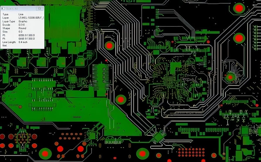
PCB-DFM

Step 1: Engineering Review

Before production, Kingda reviews the Gerber files, BOM, pick-and-place data, PCB specifications, and assembly requirements. The review focuses on component footprints, fine-pitch packages, polarity-sensitive devices, PCB manufacturability, component availability, and testing requirements. Potential issues are identified for clarification before manufacturing to reduce avoidable production delays and assembly defects.
PCB Manufacturing

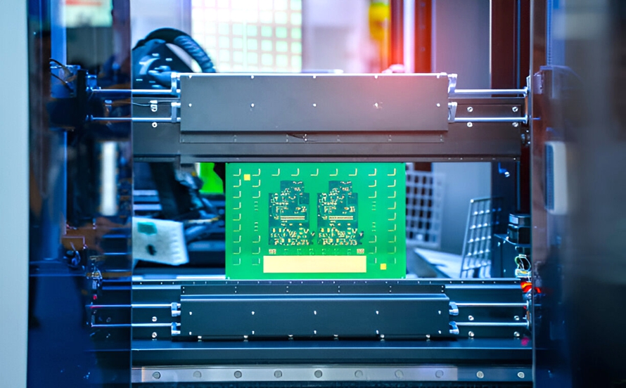
Step 2: PCB Manufacturing and Component Sourcing

The PCB is manufactured according to the approved stack-up, dimensions, copper specifications, surface finish, and other project requirements. In parallel, components are sourced against the approved BOM. Incoming materials are checked against the relevant specifications, with attention to part numbers, quantities, packaging, and visible condition. PCB manufacturing and component sourcing are coordinated to support a controlled production schedule.
SMT Assembly

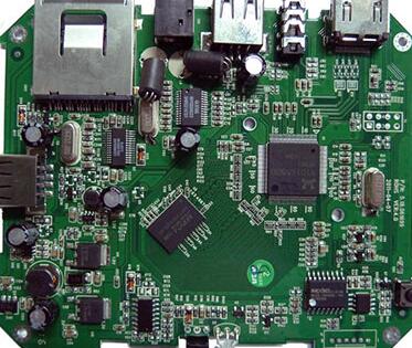
Step 3: SMT Assembly

The assembly process begins with solder paste printing, followed by Solder Paste Inspection (SPI), automated component placement, and reflow soldering. Automated Optical Inspection (AOI) is used to inspect accessible solder joints and component placement for potential defects. X-ray inspection may be applied where appropriate, particularly for hidden solder joints such as those beneath BGA packages. Through-hole assembly is performed when required by the design. Process parameters and inspection criteria are selected according to the PCB design, component packages, and customer requirements.

PCBA Testing

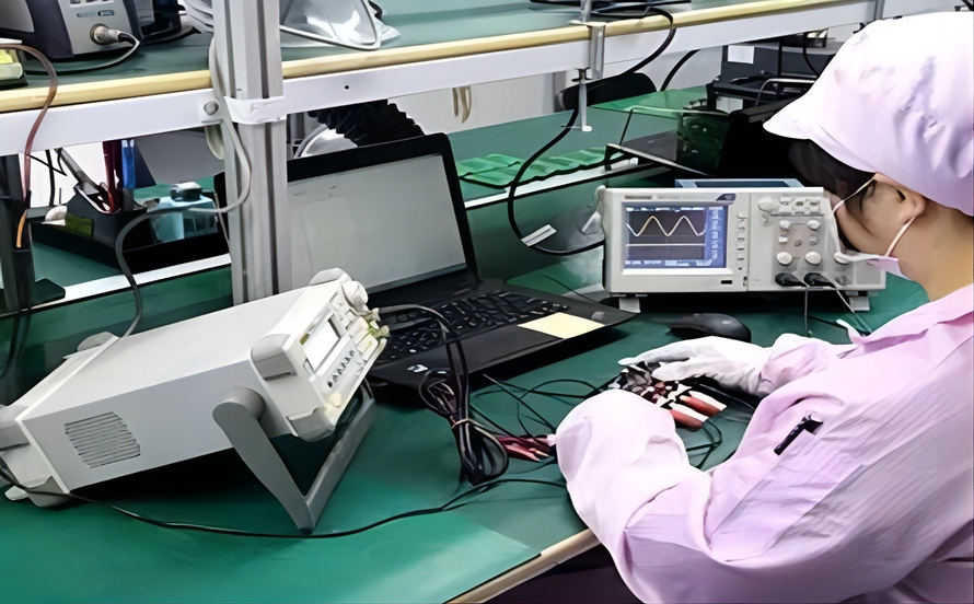
Step 4: Functional Testing

After assembly, the PCBA is tested according to the product's intended functions and customer requirements. Testing may include power verification, microcontroller programming, sensor data acquisition, wireless communication, and interface checks, depending on the product design. Functional testing helps identify electrical and assembly-related issues before final assembly or shipment.
PCB-visual-inspection

Step 5: Final Inspection and Traceability

Completed boards undergo final inspection to verify workmanship, component placement, connector condition, and compliance with the agreed acceptance criteria. Where required, inspection and test records can be maintained to support production traceability and quality review. For industrial IoT products intended for continuous operation, consistent process control and documented inspection criteria are important for maintaining quality across production batches.

Manufacturing Challenges and Solutions

Manufacturing Challenge Recommended Manufacturing Approach
High Component Density Review footprints, clearances, and placement data before production.
Fine-Pitch Soldering Control solder paste printing, placement accuracy, and reflow parameters.
Wireless Connectivity Follow RF layout requirements and verify communication functionality.
Power Stability Check power-related components and perform specified electrical tests.
Component Shortages Verify sourcing risks and obtain approval for alternatives.
Batch-to-Batch Consistency Apply defined inspection criteria and maintain relevant production records.

Project Outcome and Manufacturing Value

A successful IoT PCB assembly project requires coordination between engineering, procurement, manufacturing, and testing.

By integrating these activities within one manufacturing workflow, Kingda can help customers reduce supplier coordination, identify manufacturing risks earlier, and establish a clearer path from prototype builds to low-volume production.

For industrial IoT developers, this approach supports more controlled manufacturing preparation and provides a foundation for consistent PCBA quality as product requirements evolve.

Actual production results depend on the design, component selection, testing coverage, and agreed quality criteria.

Let’s Start Work
Together

Please feel free to contact us. We will get back to you with 1-2 business days. Or just call us now.

3rd Floor, 11th Bldg., Houting 3rd Industrial Zone, Shajing, Baoan, Shenzhen, China

Why Choose Kingda for IoT PCB Assembly?

Kingda provides One-Stop PCBA Manufacturing services for IoT and industrial electronic products, including:

From prototype builds to low-volume production, Kingda supports IoT hardware teams with coordinated manufacturing services designed around their product requirements.