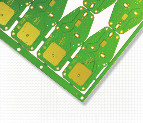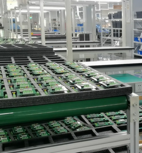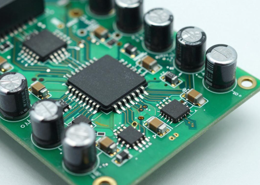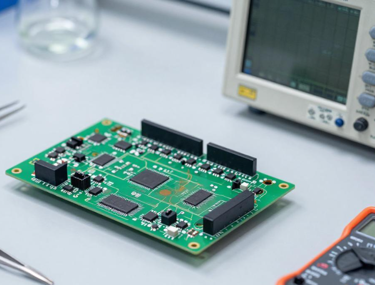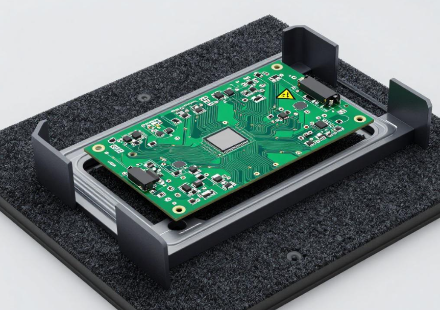
After PCB fabrication, inspection, and testing are completed, packaging becomes an important part of protecting board quality during shipment and storage. Problems such as electrostatic exposure, board-edge damage, surface scratches, warpage, moisture absorption, and compression damage may not originate from the manufacturing process itself. They can also occur during handling,…
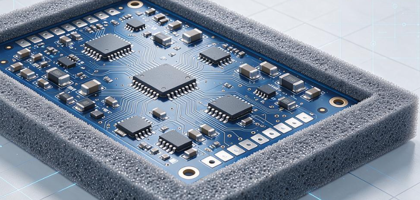
Different PCB packaging materials can provide very different levels of protection, even when they are used for the same PCB product. When packaging is evaluated only from a cost perspective, important material characteristics may be overlooked, resulting in ESD exposure, surface scratches, board deformation, damaged corners, moisture ingress, or package…
Standard 1.6 mm FR-4 PCBs generally have sufficient mechanical rigidity to tolerate conventional packaging and transportation conditions. However, thin PCB packaging requires a different approach when boards are 0.4–0.8 mm thick or have other mechanically sensitive structures. HDI boards, large-format panels, gold-finger PCBs, and thick-copper boards may also require specialized…
PCB manufacturers may encounter a recurring problem: production equipment is operating normally and the material grades have not changed, yet yield decreases during humid spring and summer conditions, while a different group of defects appears during dry and cold periods. These seasonal quality fluctuations are often associated with changes in…
Many PCB manufacturers adjust equipment and process parameters when seasons change, yet batch defects may continue to occur. One important reason is that process settings are adjusted while PCB raw materials and work-in-process materials are not managed according to changing environmental conditions. Materials such as copper-clad laminate, prepreg, and copper…
Seasonal changes can create hidden challenges for PCB manufacturing. Temperature, humidity, static electricity, material moisture, chemical-bath conditions, and equipment performance may change with the environment. If these variables are not managed systematically, a production line may experience recurring quality problems during the same season every year. A common manufacturing response…
In smart industrial transmitter development, even a well-designed schematic and carefully selected components can still result in measurement drift, signal jumps, communication errors, or unstable outputs if the PCB layout is poorly designed. An industrial transmitter is typically a mixed-signal system in which low-level sensor signals, analog conditioning circuits, digital…
Completing the schematic, PCB design, prototype fabrication, and functional debugging is only part of the development process for a smart industrial transmitter. Once a transmitter is deployed in factories, process-control systems, outdoor pipelines, or other demanding environments, PCB reliability becomes critical to long-term product performance. A prototype may perform well…
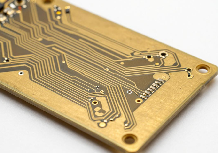
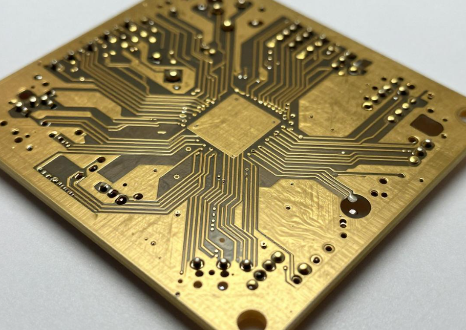
ENIG PCB technology is widely used in industrial control, automotive electronics, telecommunications, networking, and other applications that require flat contact surfaces, good solderability, and compatibility with fine-pitch packages such as BGA. However, achieving a qualified gold thickness on a prototype does not necessarily mean that the same ENIG process control…
For high-volume ENIG PCB manufacturing, gold thickness uniformity is influenced by much more than the nominal immersion-gold process time. Bath chemistry, temperature, pH, solution circulation, agitation, rack configuration, board loading density, and equipment condition all affect the chemical environment around the exposed nickel surface. During continuous production, the chemistry of…