


Copper Thickness (Copper Weight) is a highly important parameter in PCB design and manufacturing, exerting multifaceted influence on the performance and reliability of the final product.
In simple terms, copper thickness refers to the thickness of the copper layer on a PCB and is typically expressed in ounces (oz). A copper thickness of 1 oz corresponds to approximately 35 micrometers.
Major Impacts of Copper Thickness on Products
Current Carrying Capacity
The thicker the copper layer, the larger its cross-sectional area, which reduces resistance and allows for greater current flow.
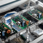
In applications that involve high power or large currents (such as power supply boards, automotive electronics, and industrial equipment), thicker copper layers (2 oz, 3 oz, or even 4 oz) are necessary to prevent overheating or damage.
Insufficient copper thickness can lead to overheating, performance degradation, and even safety risks.
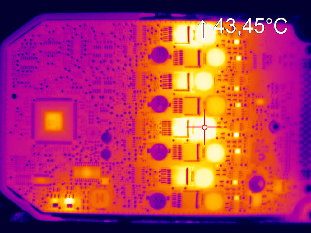
Thermal Management and Heat Dissipation
Copper layers serve not only as electrical conductors but also as thermal conductors.
Thicker copper layers offer better heat conductivity, allowing heat generated by components to be evenly distributed and preventing localized overheating.
This is especially important for high-power components such as power MOSFETs, LED arrays, and CPUs.
Current Carrying Capacity
The thicker the copper layer, the larger its cross-sectional area, which reduces resistance and allows for greater current flow.
In applications that involve high power or large currents (such as power supply boards, automotive electronics, and industrial equipment), thicker copper layers (2 oz, 3 oz, or even 4 oz) are necessary to prevent overheating or damage.
Insufficient copper thickness can lead to overheating, performance degradation, and even safety risks.
Thermal Management and Heat Dissipation
Copper layers serve not only as electrical conductors but also as thermal conductors.
Thicker copper layers offer better heat conductivity, allowing heat generated by components to be evenly distributed and preventing localized overheating.
This is especially important for high-power components such as power MOSFETs, LED arrays, and CPUs.
Mechanical Strength and Durability
Thicker copper layers enhance the overall mechanical strength of the PCB, improving resistance to tearing, bending, and wear.
In environments with frequent insertion/removal or vibration (such as automotive or aerospace applications), PCBs with thicker copper layers offer higher reliability.
Signal Integrity and Electrical Characteristics
Variations in copper thickness affect the resistance and inductance of conductors, which in turn influence the transmission characteristics of high-frequency signals.
In high-speed signal designs, it is essential to precisely control copper thickness to ensure impedance matching and minimize signal reflection.
If the copper is made too thick without adjusting the design accordingly, the impedance may deviate from the intended value.
Manufacturing Costs and Process Requirements
The thicker the copper layer, the higher the cost and the greater the processing difficulty.
PCBs with thick copper layers require more precise etching control to ensure trace width and spacing accuracy.
Processes such as reflow soldering and drilling also become more complex, potentially increasing production time and defect rates.
Design Flexibility
Thinner copper layers (less than 1 oz) are suitable for fine-pitch wiring and high-density designs.
Thicker copper layers (2 oz and above) are appropriate for power and ground planes or traces carrying large currents, but the designer must balance signal density and current capacity.
As such, copper thickness impacts PCB performance, reliability, and cost, making it essential to choose the optimal thickness according to the application.
If adjustments are required to meet specific technical requirements, please feel free to consult with us.