


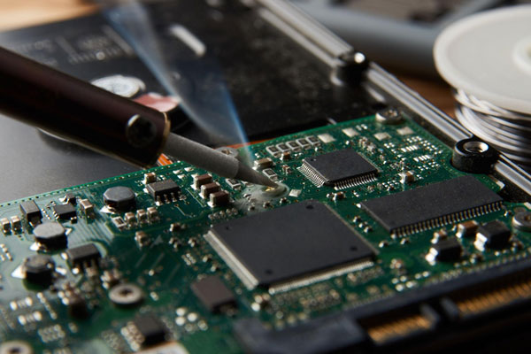
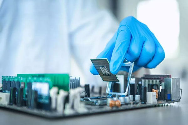
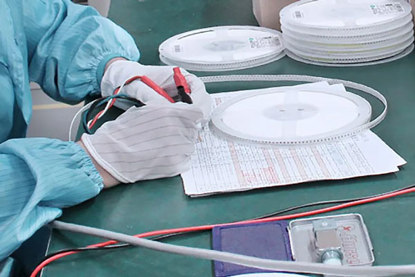
Power Device Soldering Reliability
High-current components are vulnerable to cold solder joints, solder fatigue, and long-term reliability failures.
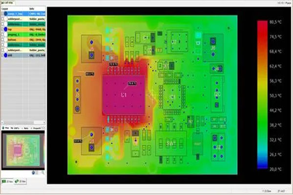
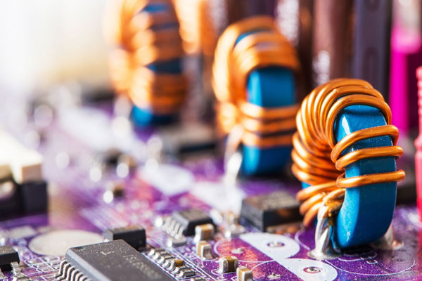
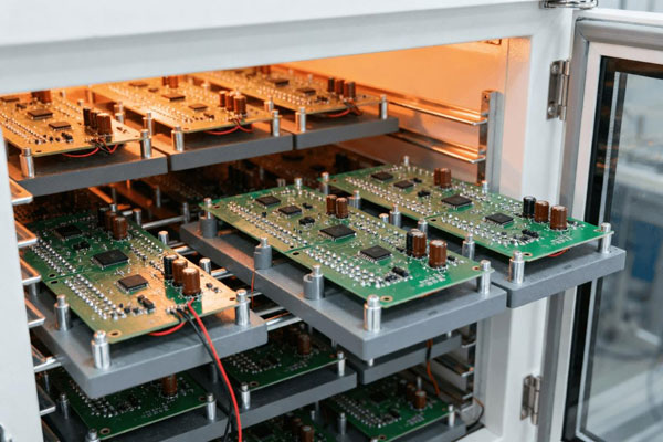
Thermal & Heat Management
High-power electronics generate excessive heat, increasing risks of thermal instability and product degradation.
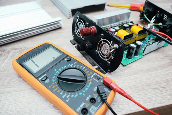
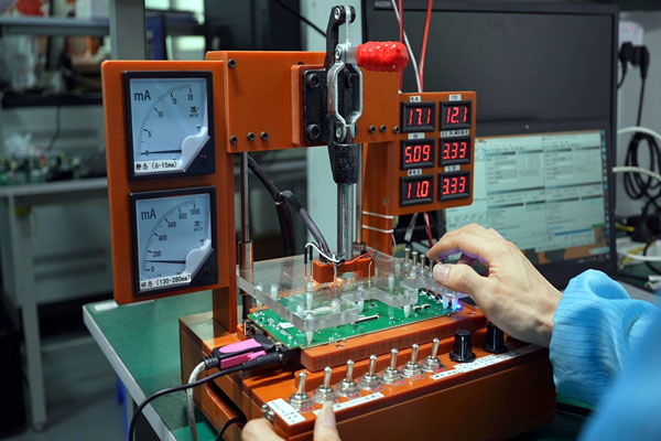
Incomplete Testing & Validation
Limited testing coverage and manual inspection may reduce product consistency and increase quality risks.
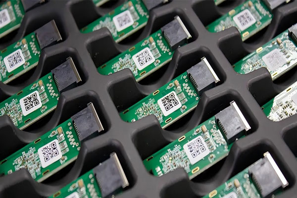
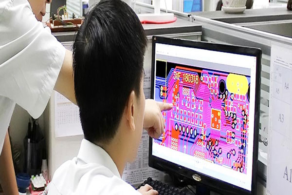
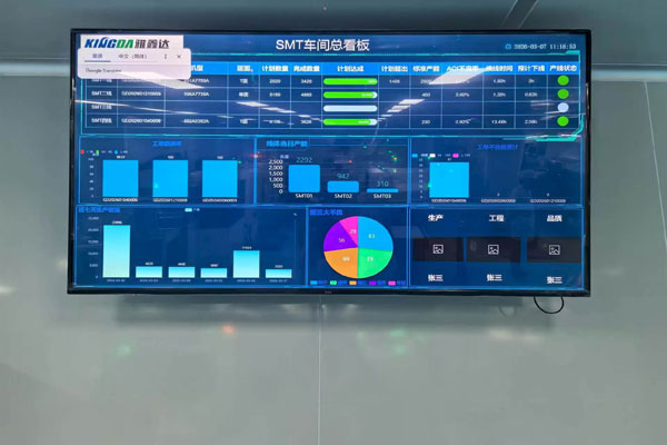
Limited Manufacturing Traceability
Frequent engineering changes and repeated pilot production issues slow down commercialization.
Slow New Product Introduction (NPI)
Frequent process modifications, engineering coordination gaps, and repeated pilot production issues often slow down product commercialization.
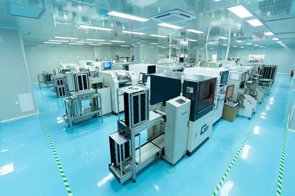
Supply Chain & Production Stability
Component shortages, substitutions, and unstable lead times create pressure on delivery continuity.
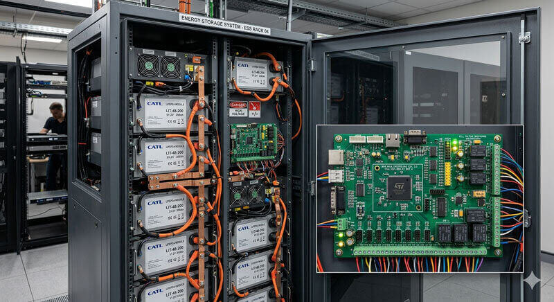
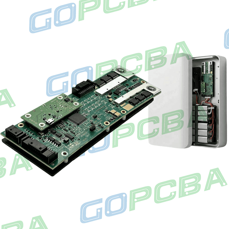
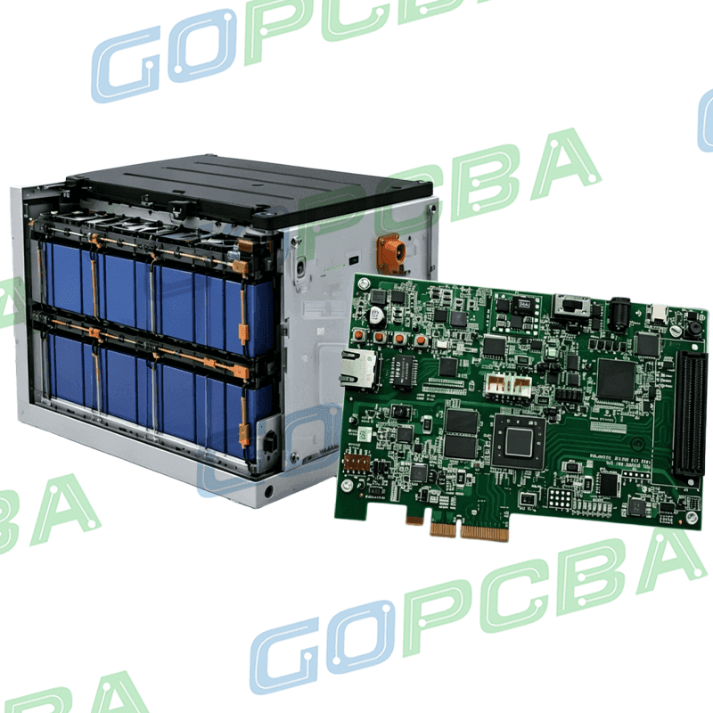
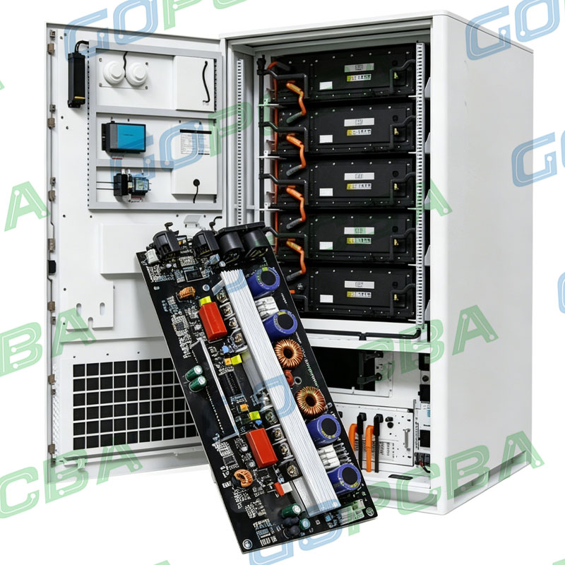
Energy Storage Systems (ESS / BMS)
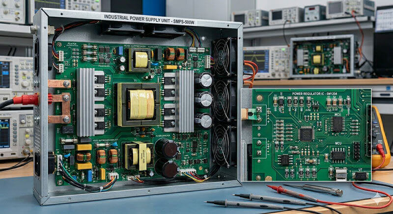
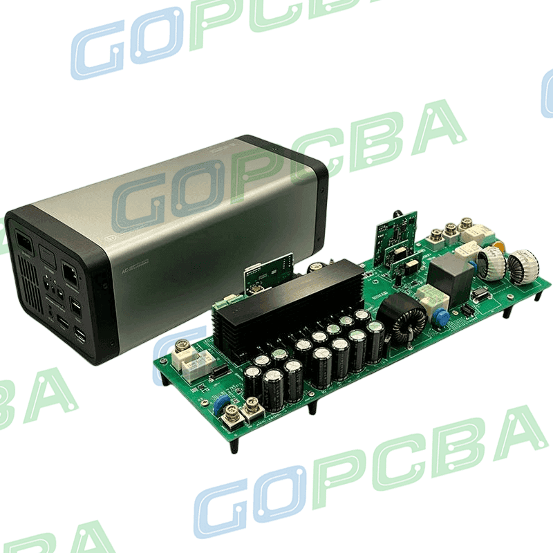
Power Supply & Industrial Power
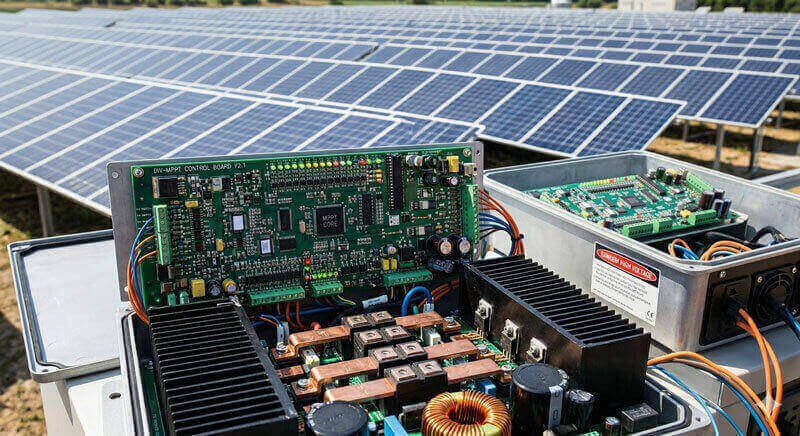
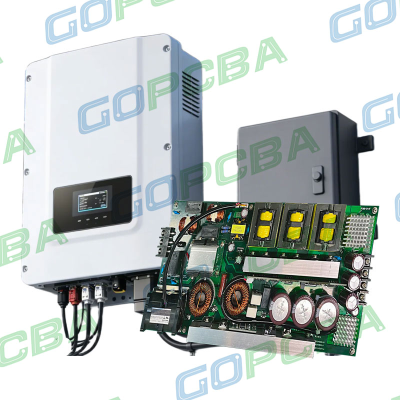
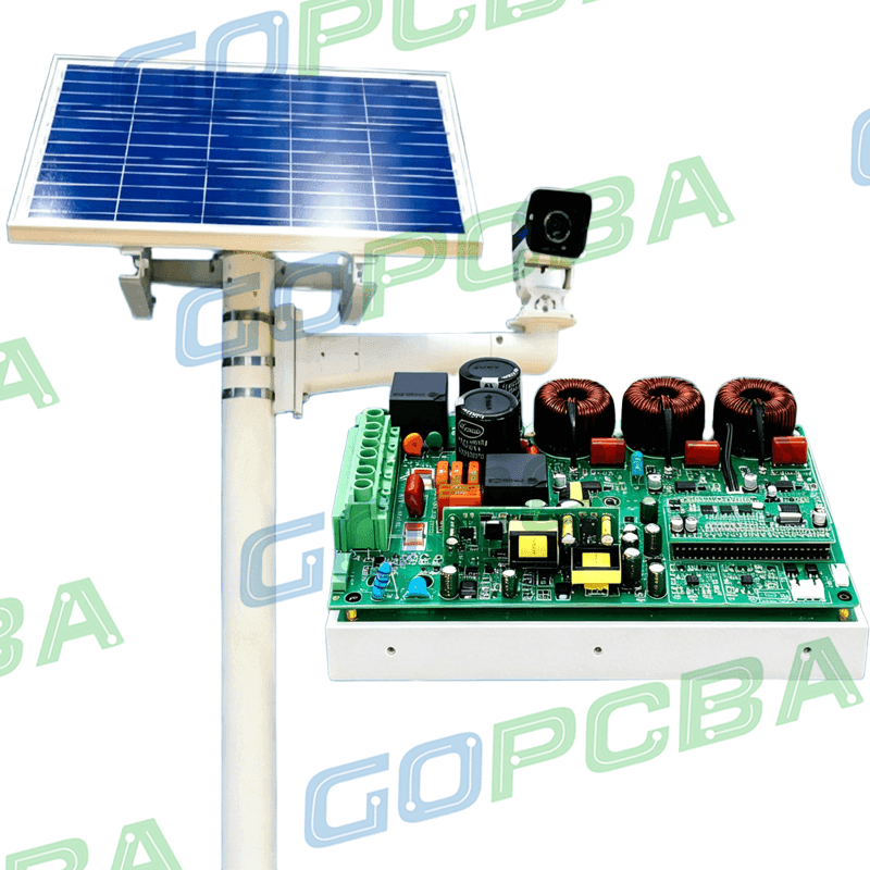
Solar & Inverter Systems
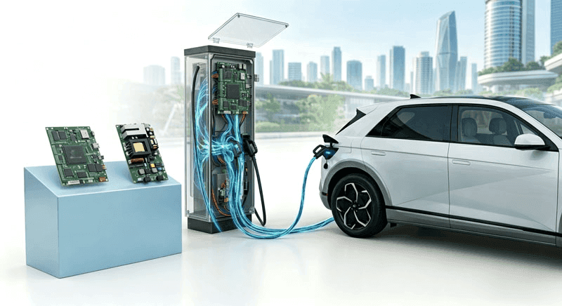
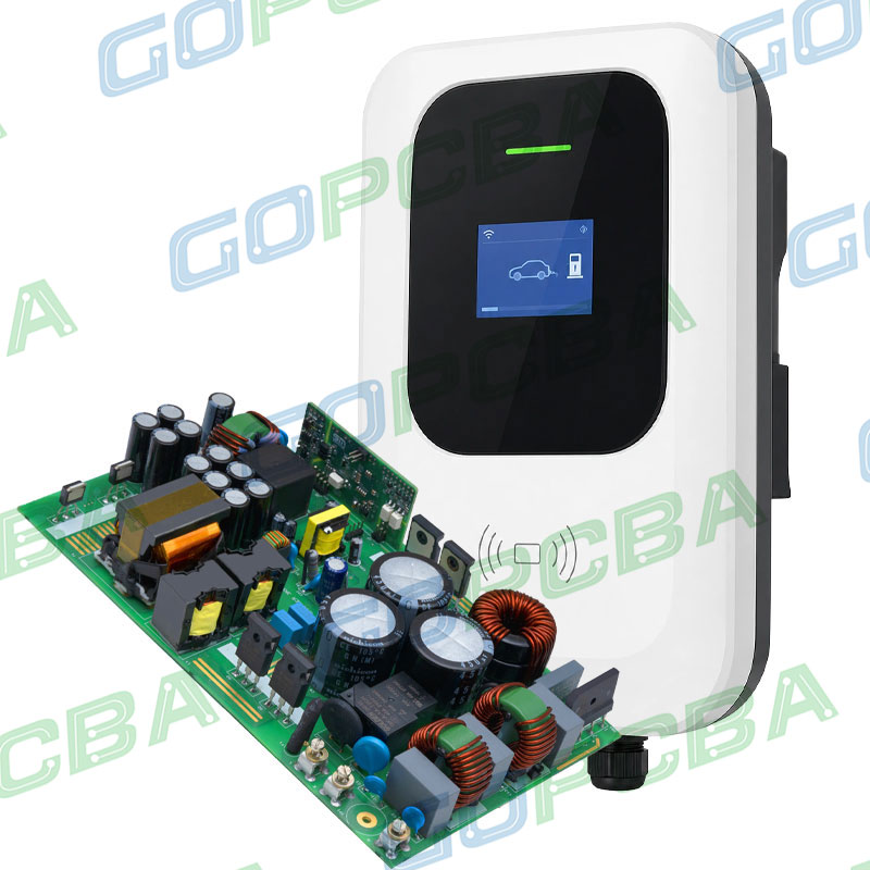
EV Charging Systems