


Engineering Context
PCB assembly services form the critical bridge between electronic design intent and reliable product realization. As electronic systems evolve toward higher integration, higher frequencies, and stricter reliability requirements, PCB assembly is no longer a purely manufacturing task but an engineering-controlled process that directly impacts electrical performance, thermal behavior, and long-term system stability.
Modern PCB assembly services must support diverse applications ranging from industrial control and medical electronics to automotive systems, RF communication equipment, and high-speed digital platforms. This article analyzes PCB assembly services from an engineering perspective, focusing on process selection, material compatibility, stackup interaction, and validation methodologies required to achieve consistent and reliable assemblies.
Core Engineering Challenges
Providing robust PCB assembly services involves addressing multiple interrelated engineering challenges.
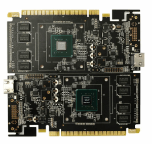
Process diversity and compatibility is a primary challenge. A single PCB assembly may integrate SMT components, through-hole devices, fine-pitch packages, power modules, and RF connectors. Each assembly technology introduces unique thermal and mechanical constraints that must be managed within a unified process flow.
Signal and power integrity preservation is increasingly critical. Assembly-related variables such as solder joint geometry, component placement accuracy, and via quality can affect impedance continuity, return paths, and power delivery stability, particularly in high-speed digital and RF PCB designs.
Thermal stress and mechanical reliability also pose challenges. Reflow profiles, wave solder temperatures, and selective soldering processes must be optimized to avoid pad lifting, barrel cracking, or component damage, especially on multilayer and mixed-material PCBs.
Finally, EMI control and regulatory compliance depend heavily on assembly execution. Improper grounding, inconsistent solder joints, or assembly-induced warpage can degrade shielding effectiveness and compromise electromagnetic compatibility.
Material Science & Dielectric Performance
Although PCB assembly services focus on manufacturing, material science plays a foundational role in assembly quality and long-term reliability.
Assembly processes must be matched to PCB laminate properties, including Tg, CTE, copper thickness, and surface finish. High-Tg FR-4 materials are commonly used for general electronics, while RF PCB materials and hybrid stackups require tighter thermal profile control during reflow.
Typical Material Considerations in PCB Assembly
| Parameter | Typical Range | Engineering Impact |
|---|---|---|
| Glass Transition (Tg) | 150–180 °C | Reflow thermal margin |
| Z-axis CTE | ≤70 ppm/°C | Via reliability |
| Copper Weight | 0.5–3 oz | Thermal and current handling |
| Surface Finish | ENIG, ENEPIG, OSP | Solderability consistency |
| Dielectric Stability | Application-dependent | Signal integrity |
Material compatibility ensures that solder joints, vias, and laminate interfaces remain stable throughout multiple thermal excursions, including assembly, rework, and field operation.
GOPCBA Case Study — Industrial and Communication PCB Assembly
Customer Background
A system integrator developing industrial control and communication equipment required scalable PCB assembly services capable of supporting both prototype and volume production. The assemblies included mixed SMT and through-hole components, power electronics, and communication interfaces with moderate RF sensitivity.
Engineering Problems
-
Inconsistent solder joint quality across mixed-technology boards
-
Power rail instability caused by assembly-induced parasitics
-
EMI issues linked to grounding and connector soldering
-
Yield loss during early production ramps
GOPCBA Solution
GOPCBA delivered an engineering-controlled PCB assembly service emphasizing process definition, material matching, and inspection strategy. SMT reflow profiles were tailored to laminate Tg and copper distribution, while selective soldering was applied to high-mass through-hole components.
Assembly design reviews focused on component placement, grounding strategy, and manufacturability improvements. Automated optical inspection and X-ray inspection were used to validate solder joint integrity and detect hidden defects.
Measured Performance Results
| Test Item | Requirement | Measured Result |
|---|---|---|
| SMT Placement Accuracy | ±50 µm | ±28 µm |
| Solder Joint Defect Rate | ≤0.5% | 0.18% |
| Power Ripple Reduction | Target ≥20% | 32% |
| Assembly Yield | ≥98% | 99.3% |
The optimized PCB assembly services enabled stable ramp-up from prototype to production while maintaining electrical and mechanical reliability.
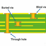
Stackup Design & RF Implementation
While stackup design is typically defined during PCB fabrication, PCB assembly services must account for stackup-related constraints to ensure successful assembly and performance preservation.
Example Stackup for Mixed-Technology PCB Assembly
| Layer | Function | Material |
|---|---|---|
| L1 | SMT Components / Signals | FR-4 or RF Laminate |
| L2 | Solid Ground Plane | Copper |
| L3 | Power Plane | Copper |
| L4 | Control / High-Speed Signals | FR-4 |
| L5 | Ground Plane | Copper |
| L6 | Through-Hole Components | FR-4 |
This stackup supports short return paths, effective EMI suppression, and balanced thermal behavior during assembly. For RF PCB assembly, controlled impedance traces and continuous reference planes are preserved throughout soldering and rework.
Simulation tools such as ADS, TDR analysis, and power integrity simulation are used to assess assembly-related impacts on signal integrity and impedance continuity.
Environmental & Reliability Validation
High-quality PCB assembly services include structured validation to confirm long-term reliability under real-world operating conditions.
Reliability Test Summary
| Test Type | Condition | Result |
|---|---|---|
| Thermal Cycling | −40 °C ↔ 125 °C, 500 cycles | Pass |
| High-Temp Operating Life | 105 °C, 1000 hrs | Pass |
| Humidity Exposure | 85 °C / 85% RH | Pass |
| Vibration | Application-specific | Pass |
| Solder Reflow Endurance | Multiple profiles | No degradation |
Thermal FEM analysis supports heat dissipation optimization for power components, while post-test cross-section analysis verifies solder joint integrity and via reliability.
Engineering Summary & Contact
PCB assembly services play a decisive role in determining the electrical performance, mechanical robustness, and reliability of electronic systems. An engineering-driven approach that integrates material understanding, process control, stackup awareness, and rigorous validation is essential for delivering consistent and high-quality PCB assemblies.
From SMT and through-hole assembly to mixed-technology integration and reliability testing, comprehensive PCB assembly services enable electronics manufacturers to achieve predictable performance and long service life across industrial, medical, automotive, and communication applications. GOPCBA provides engineering-focused PCB assembly services designed to support high-reliability electronic products from prototype development through volume production.