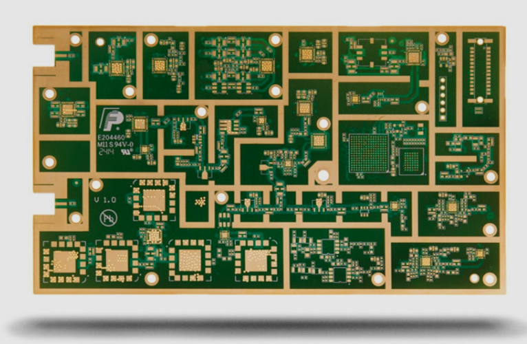
Low Loss PCB Laminate Material: Complete 2026 Engineering Guide Low loss PCB laminate material is engineered to minimize dielectric loss and signal attenuation at high frequencies — typically with a dissipation factor (Df) below 0.010 at 10 GHz. For 5G mmWave, AI servers running 112G PAM4, and radar systems, ultra-low-loss…
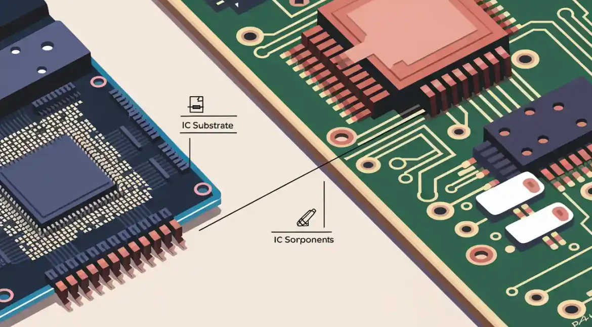
PCB Layout Design Services for High-Speed and HDI PCBs PCB layout design is the process of transforming an electrical schematic into a physical printed circuit board (PCB) layout that meets the required electrical, mechanical, manufacturing, and performance requirements. A well-designed PCB layout not only ensures reliable electrical connections but can…
In modern high-speed electronic devices, PCB impedance plays a critical role in system stability, data integrity, and product lifespan. As clock frequencies rise and digital signal edges become steeper, the printed circuit board is no longer a passive element—it effectively becomes part of the transmission line. Proper PCB impedance control…