


Engineering Context
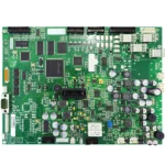
Industrial IoT gateways serve as the critical interface between field-level sensors, industrial networks, and cloud-based analytics platforms. These gateways integrate multiple communication technologies, including industrial Ethernet, wireless interfaces, and fieldbus protocols, within compact enclosures deployed in electrically noisy and environmentally harsh industrial environments. The industrial PCB assembly used in such gateways must therefore achieve robust EMI control while maintaining long-term electrical and mechanical reliability.
Unlike consumer IoT devices, industrial IoT gateways are expected to operate continuously for years, often in proximity to motors, inverters, and switching power supplies. Assembly-related factors—such as grounding continuity, solder joint consistency, component placement accuracy, and thermal process control—play a decisive role in EMI performance and lifecycle stability. This article examines how an engineering-driven industrial PCB assembly approach enables effective EMI control and long-term reliability in Industrial IoT gateway platforms.

Core Engineering Challenges
Industrial IoT gateway PCB assemblies encounter a convergence of RF, digital, and power electronics challenges.
EMI generation and susceptibility are among the most critical issues. High-speed digital interfaces, DC-DC converters, and RF transceivers coexist on the same PCB, creating multiple potential sources of conducted and radiated emissions. Assembly inconsistencies can worsen return path discontinuities and ground impedance, increasing EMI risk.
Long-term reliability under continuous operation is another key challenge. Industrial IoT gateways often operate 24/7 in sealed enclosures, subject to elevated ambient temperatures and limited airflow. Solder joints, vias, and laminate interfaces must remain stable under prolonged thermal stress.
Mechanical stress and environmental exposure further complicate assembly requirements. Vibration from nearby machinery and exposure to humidity or industrial contaminants can accelerate degradation if assembly quality is not robust.
Finally, process repeatability across production volumes is essential. Industrial IoT deployments require consistent performance across thousands of units, making controlled and repeatable PCB assembly processes a necessity.
Material Science & Dielectric Performance
Material selection underpins both EMI behavior and long-term reliability in industrial PCB assembly for IoT gateways.
High-Tg FR-4 materials are typically used for the core stackup due to their mechanical robustness and thermal stability. For RF sections supporting wireless communication, localized RF PCB materials with controlled dielectric properties may be incorporated to preserve signal integrity and reduce insertion loss.
Typical Material Parameters for Industrial IoT Gateway PCB Assembly
| Parameter | Typical Value | Engineering Impact |
|---|---|---|
| Dielectric Constant (Dk) | 3.8 – 4.4 | Controlled impedance |
| Dissipation Factor (Df) | ≤0.015 | Reduced RF loss |
| Glass Transition (Tg) | ≥170 °C | Thermal endurance |
| Z-axis CTE | ≤70 ppm/°C | Via reliability |
| Surface Finish | ENIG / ENEPIG | Solder joint consistency |
Stable dielectric performance supports predictable impedance for high-speed and RF signals, while low Z-axis CTE minimizes stress accumulation during thermal cycling. Material compatibility with assembly processes ensures consistent solder joint formation and reduced risk of latent defects.
GOPCBA Case Study — Industrial IoT Gateway PCB
Customer Background
A provider of industrial IoT gateway solutions required an industrial PCB assembly capable of supporting Ethernet, wireless communication, and multiple fieldbus interfaces. The gateway was intended for deployment in factory environments with high EMI exposure and long service life requirements.
Engineering Problems
-
EMI emissions exceeding regulatory limits during pre-compliance testing
-
Intermittent communication errors under high electrical noise
-
Thermal stress around power management components
-
Reliability concerns during extended burn-in testing
GOPCBA Solution
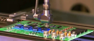
GOPCBA delivered an engineering-focused industrial PCB assembly solution emphasizing EMI control and reliability. Assembly process optimization began with a detailed review of grounding strategy, component placement, and solder joint geometry.
Controlled solder paste volumes and refined reflow profiles ensured uniform ground connections and minimized impedance discontinuities. Shielded RF components and connectors were assembled with reinforced grounding to reduce radiated emissions.
Thermal management was addressed through optimized component placement and improved solder joint thermal conductivity. Design-for-assembly adjustments reduced stress concentration around connectors and large components.
Measured Performance Results
| Test Item | Requirement | Measured Result |
|---|---|---|
| EMI Margin | ≥6 dB | 12 dB |
| Ethernet Packet Error Rate | ≤10⁻¹² | <10⁻¹⁴ |
| Power Rail Ripple | ≤50 mV | 21 mV |
| Assembly Yield | ≥98% | 99.2% |
The optimized industrial PCB assembly achieved stable EMI performance and reliable operation under simulated industrial conditions.
Stackup Design & RF Implementation
Stackup design strongly influences EMI control and assembly stability in industrial IoT gateway PCBs.
Example Stackup for Industrial IoT Gateway PCB
| Layer | Function | Material |
|---|---|---|
| L1 | High-Speed / RF Signals | FR-4 / RF Laminate |
| L2 | Solid Ground Plane | Copper |
| L3 | Power Plane | Copper |
| L4 | Control and Low-Speed Signals | High-Tg FR-4 |
| L5 | Ground Plane | Copper |
| L6 | Bottom Components | High-Tg FR-4 |
This stackup ensures continuous reference planes for high-speed and RF traces, reducing loop area and EMI emissions. Balanced copper distribution improves mechanical stability during reflow and reduces warpage, supporting precise component placement.
EMI and signal integrity simulations using ADS validated controlled impedance and minimized crosstalk. TDR measurements confirmed impedance consistency after assembly. Thermal FEM analysis supported heat spreading optimization around power components.
Environmental & Reliability Validation
Industrial IoT gateway PCB assemblies must pass comprehensive validation to ensure long-term reliability in harsh environments.
Reliability Test Summary
| Test Type | Condition | Result |
|---|---|---|
| Thermal Cycling | −40 °C ↔ 85 °C, 500 cycles | Pass |
| High-Temp Operating Life | 85 °C, 1000 hrs | Pass |
| Humidity Exposure | 85 °C / 85% RH | Pass |
| Vibration | Industrial profile | Pass |
| Solder Reflow Endurance | Multiple profiles | No degradation |
Post-test inspections confirmed stable solder joints and intact via barrels. Thermal FEM correlation with measured data demonstrated effective heat distribution, reducing stress accumulation over long-term operation.
Engineering Summary & Contact
Achieving effective EMI control and long-term reliability in is essential for Industrial IoT gateways operating in electrically noisy and environmentally demanding conditions. By in industrial PCB assembly tegrating material understanding, optimized stackup design, precise assembly processes, and rigorous validation, industrial PCB assemblies can deliver stable communication performance and extended service life.
An engineering-driven approach to industrial PCB assembly minimizes EMI risk, enhances mechanical and thermal robustness, and ensures consistent manufacturing quality across production volumes. GOPCBA provides industrial PCB assembly services focused on EMI control, reliability validation, and process precision to support Industrial IoT gateway platforms in modern industrial ecosystems.