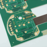


Engineering Context
High-speed communication modules are fundamental components in modern networking equipment, data transmission systems, and industrial communication platforms. These modules integrate high-speed processors, RF interfaces, power management circuits, and dense interconnect structures within compact form factors. In such architectures, SMT PCB assembly is no longer a purely mechanical manufacturing step, but a critical engineering process that directly affects signal integrity, electromagnetic performance, and long-term reliability.
As data rates continue to increase and channel margins shrink, even minor assembly-induced variations—such as solder joint geometry, component placement accuracy, and laminate warpage—can introduce impedance discontinuities, insertion loss variation, and phase distortion. This article examines how engineering-driven SMT PCB assembly improves signal integrity and assembly precision in high-speed communication modules, integrating material science, stackup design, simulation, and environmental validation.

Core Engineering Challenges
High-speed communication modules present tightly coupled electrical and manufacturing challenges.
Signal integrity sensitivity is a primary issue. High-speed differential pairs, RF interfaces, and clock distribution networks are extremely sensitive to impedance variation, parasitic inductance, and discontinuities introduced during assembly. Variations in solder joint shape or component coplanarity can create localized impedance mismatches that degrade eye diagrams and increase bit error rates.
Assembly precision requirements are increasingly stringent. Fine-pitch packages, micro-BGAs, and high-density connectors demand micron-level placement accuracy and controlled solder volume. Any misalignment can affect electrical continuity and mechanical reliability.
EMI and crosstalk control becomes more difficult as integration density increases. Inadequate grounding continuity or inconsistent return paths caused by assembly defects can amplify radiated and conducted emissions.
Thermal stress management further complicates assembly. High-speed processors and RF ICs generate localized heat, and uneven thermal profiles during reflow can induce warpage, solder joint voiding, and long-term reliability risks.
Material Science & Dielectric Performance
Material selection establishes the electrical foundation for SMT PCB assembly in high-speed communication modules.
Low-loss RF PCB materials and high-performance FR-4 laminates with controlled dielectric properties are commonly used to preserve signal integrity. Stable dielectric constant (Dk) ensures predictable impedance, while low dissipation factor (Df) reduces insertion loss and signal attenuation at higher frequencies.
Copper foil roughness also plays a critical role. Smoother copper profiles reduce conductor loss and improve high-frequency performance, contributing to better signal margins.
Typical Material Parameters for High-Speed SMT PCB Assembly
| Parameter | Typical Value | Engineering Impact |
|---|---|---|
| Dielectric Constant (Dk) | 3.4 – 3.8 | Controlled impedance |
| Dissipation Factor (Df) | ≤0.008 | Low insertion loss |
| Glass Transition (Tg) | ≥170 °C | Thermal stability |
| Z-axis CTE | ≤60 ppm/°C | Via reliability |
| Copper Profile | Low-roughness | Reduced conductor loss |
Material consistency ensures that assembly-induced variations do not compound dielectric-related signal degradation.
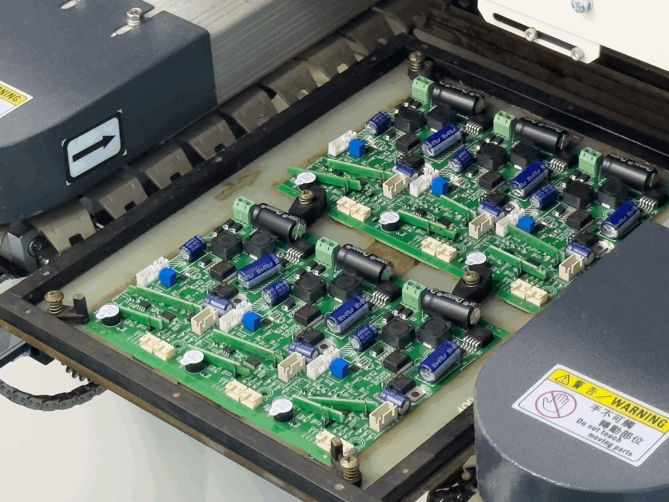
GOPCBA Case Study — High-Speed Communication Module PCB
Customer Background
A manufacturer of high-speed communication modules for industrial networking and data transmission systems required an SMT PCB assembly solution capable of supporting multi-gigabit data rates. The module integrated high-speed processors, RF interfaces, memory devices, and power management circuits within a compact multilayer PCB.
Engineering Problems
-
Eye diagram degradation during system validation
-
Impedance discontinuities near high-speed connectors
-
EMI emissions exceeding pre-compliance limits
-
Assembly yield losses due to fine-pitch BGA defects
GOPCBA Solution
GOPCBA implemented a signal-integrity-driven SMT PCB assembly strategy. Precision stencil design and controlled solder paste deposition ensured consistent solder joint geometry across fine-pitch components.
Reflow profiles were optimized to match laminate Tg and copper distribution, minimizing warpage and solder joint voiding. Component placement accuracy was enhanced through advanced vision alignment and coplanarity control.
Design-for-assembly reviews focused on high-speed connector anchoring and return path continuity. Grounding structures were reinforced to maintain stable reference planes across the assembled PCB.
Measured Performance Results
| Test Item | Requirement | Measured Result |
|---|---|---|
| Impedance Deviation | ±10% | ±4.8% |
| Insertion Loss (2.5 GHz) | ≤ −1.8 dB | −1.3 dB |
| EMI Margin | ≥6 dB | 10.5 dB |
| SMT Defect Rate | ≤0.5% | 0.14% |
| Assembly Yield | ≥98% | 99.6% |
The optimized SMT PCB assembly demonstrated clear improvements in signal integrity and manufacturing precision.
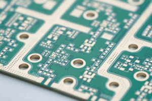
Stackup Design & RF Implementation
Stackup design is fundamental to both signal integrity and assembly stability in high-speed SMT PCB assemblies.
Example Stackup for High-Speed Communication Module
| Layer | Function | Material |
|---|---|---|
| L1 | High-Speed Signals / Components | Low-Loss Laminate |
| L2 | Solid Ground Plane | Copper |
| L3 | Power Plane | Copper |
| L4 | High-Speed Signals | Low-Loss Laminate |
| L5 | Ground Plane | Copper |
| L6 | Control / Low-Speed Signals | High-Tg FR-4 |
This stackup provides continuous reference planes for differential pairs and RF traces, reducing impedance discontinuities and EMI coupling. Balanced copper distribution improves mechanical stability during reflow, supporting precise assembly.
Electromagnetic simulations using ADS and impedance verification via TDR measurements confirmed controlled impedance and minimal phase distortion after assembly. Thermal FEM analysis supported heat spreading optimization around high-power devices.
Environmental & Reliability Validation
High-speed communication modules require robust reliability validation to ensure long-term performance stability.
Reliability Test Summary
| Test Type | Condition | Result |
|---|---|---|
| Thermal Cycling | −40 °C ↔ 85 °C, 500 cycles | Pass |
| High-Temp Operating Life | 85 °C, 1000 hrs | Pass |
| Humidity Exposure | 85 °C / 85% RH | Pass |
| Vibration | Communication equipment profile | Pass |
| Solder Reflow Endurance | Multiple profiles | No degradation |
Post-test inspections confirmed stable solder joints and intact via structures. Signal integrity testing after environmental exposure showed no measurable degradation in insertion loss or impedance consistency.
Engineering Summary & Contact
Improving signal integrity and assembly precision in SMT PCB assembly is essential for high-speed communication modules where electrical margins are limited and reliability requirements are stringent. By integrating stable dielectric materials, optimized stackup design, precise assembly processes, and comprehensive validation, SMT PCB assemblies can achieve predictable performance and long-term reliability.
An engineering-driven approach to SMT PCB assembly minimizes assembly-induced signal degradation, enhances EMI control, and ensures repeatable manufacturing quality. GOPCBA provides SMT PCB assembly services focused on signal integrity optimization, precision manufacturing, and reliability validation for high-speed communication modules and advanced electronic systems.