What Is the PCB Manufacturing Process? A Complete Guide to PCB Fabrication
Printed Circuit Boards (PCBs) are the foundation of modern electronic products and play a critical role in almost every electronic device, including consumer electronics, automotive systems, industrial equipment, medical devices, aerospace applications, and communication systems.
As the physical platform that supports electronic components and provides reliable electrical connections, PCBs directly affect the performance, reliability, signal integrity, and service life of electronic products.
The PCB manufacturing process is a highly precise and complex multi-stage production procedure involving numerous advanced technologies. From raw material preparation and inner-layer circuit fabrication to lamination, drilling, copper plating, solder mask coating, surface finishing, electrical testing, and final inspection, every manufacturing step requires strict process control and quality management.
For electronic manufacturers, engineers, and purchasing teams, understanding the complete PCB fabrication process helps optimize PCB design for manufacturability, improve product reliability, reduce production risks, and select a reliable PCB manufacturer.
This article provides a comprehensive overview of the major steps involved in PCB manufacturing, with a focus on the fabrication process of multilayer printed circuit boards.
Overview of the PCB Manufacturing Process
The specific manufacturing steps depend on the type and complexity of the circuit board, including single-sided PCBs, double-sided PCBs, multilayer PCBs, HDI PCBs, rigid-flex PCBs, and other customized circuit board solutions.
For a typical multilayer PCB manufacturing process, the production workflow can generally be summarized as follows:
PCB Design → Engineering Review → Material Preparation → Inner Layer Fabrication → AOI Inspection → Lamination → CNC Drilling → Hole Metallization → Outer Layer Circuit Formation → Solder Mask Application → Surface Finish → Silkscreen Printing → Electrical Testing → Final Inspection → Routing/V-Cut → Packaging
Each stage plays an essential role in ensuring that the final printed circuit board meets required electrical performance, mechanical strength, dimensional accuracy, and reliability standards.
1. PCB Design and Engineering Review
Before physical production begins, the PCB manufacturer receives design data from customers, including:
- Gerber files
- ODB++ files
- Drill files
- Layer stack-up information
- Material specifications
- Copper thickness requirements
- Impedance control requirements
- PCB dimensions and tolerances
Before entering mass production, experienced engineering teams perform a comprehensive Design for Manufacturability (DFM) review to identify potential manufacturing challenges and optimize the design for stable production.
The key DFM inspection items include:
- Trace width and spacing
- Via structure and hole size
- Copper thickness
- PCB layer stack-up
- Controlled impedance design
- Annular ring requirements
- Solder mask clearance
- Board dimensions and tolerance control
- Component pad geometry
A professional DFM analysis can significantly reduce manufacturing risks, improve production yield, shorten delivery cycles, and prevent unnecessary production delays.
For high-performance applications such as high-speed communication equipment, automotive electronics, and industrial control systems, accurate PCB design verification is especially important because even minor design errors may affect signal integrity and product reliability.
2. PCB Material Preparation and Copper Clad Laminate Cutting
The PCB manufacturing process begins with the preparation of raw PCB materials.
The most commonly used PCB substrate materials include:
- FR-4 PCB material
- High-Tg PCB materials
- Halogen-free PCB materials
- Polyimide materials
- PTFE-based high-frequency materials
- Metal core PCB materials
Among them, FR-4 PCB remains the most widely used substrate due to its excellent mechanical strength, thermal stability, electrical insulation properties, and cost-effectiveness.
During production, copper-clad laminates (CCL) are cut into production panels according to the required PCB dimensions.
Before circuit imaging, the copper surface undergoes cleaning and surface preparation processes to remove:
- Dust
- Oxidation
- Oil contamination
- Fingerprints
- Other surface residues
Proper surface treatment is essential because it improves the adhesion of dry film photoresist and ensures accurate circuit pattern transfer during the imaging process.
3. Inner Layer Circuit Fabrication
For multilayer circuit boards, inner-layer manufacturing is one of the most critical stages in the entire PCB fabrication process.
The main steps include:
3.1 Inner Layer Cleaning
The copper surface is cleaned and chemically treated to ensure excellent adhesion between copper and photoresist materials.
3.2 Photoresist Coating
A layer of photosensitive dry film is laminated onto the copper surface.
The dry film acts as a protective layer that defines the circuit pattern during the exposure process.
3.3 Circuit Pattern Imaging
Using high-precision photolithography equipment, the designed circuit image is transferred onto the copper layer.
The exposed areas of the dry film are hardened, while the unexposed areas are removed during development.
3.4 Etching Process
The unwanted copper areas are chemically removed, leaving only the required circuit traces.
This creates the internal conductive patterns of the multilayer PCB.
3.5 Inner Layer Inspection
After etching, automated optical inspection (AOI) equipment checks the inner layers for defects, including:
- Open circuits
- Short circuits
- Missing traces
- Excess copper
- Line width deviations
Early detection of inner-layer defects is essential because internal problems cannot be easily repaired after PCB lamination.
For a multilayer PCB, the inner layers form the internal electrical network that connects different components and PCB layers.
A typical inner-layer fabrication process includes:
Cleaning → Dry Film Lamination → UV Exposure → Developing → Etching → Dry Film Stripping → AOI Inspection
Dry Film Lamination
A photosensitive dry film is laminated onto the copper surface.
The dry film acts as a temporary protective layer during circuit pattern formation.
Exposure
The PCB artwork is transferred to the dry film using ultraviolet light.
The exposure process determines which areas of the dry film remain protected during subsequent chemical processing.
Developing
The exposed panel is chemically developed to remove the appropriate areas of the photosensitive dry film and reveal the copper areas that need to be processed.
Etching
The exposed copper is chemically etched away, leaving the designed circuit pattern.
Stripping
After etching, the remaining dry film is removed, revealing the completed inner-layer circuitry.
4. AOI Inspection
After inner-layer circuit formation, Automated Optical Inspection (AOI) is used to check the circuit pattern.
AOI systems compare the manufactured circuit against the original design data to identify potential defects such as:
- Open circuits
- Short circuits
- Missing traces
- Excess copper
- Insufficient copper
- Pattern deformation
- Incorrect circuit geometry
Early detection of inner-layer defects is particularly important because the internal circuits become inaccessible after lamination.
5. Inner-Layer Oxide Treatment and Lamination
Once the inner layers have passed inspection, they are prepared for lamination.
Brown Oxide Treatment
The copper surface is chemically treated to improve surface roughness, adhesion, and bonding performance.
This treatment helps ensure reliable bonding between copper layers and prepreg (PP) materials.
Layer Stacking
The inner-layer cores, prepreg sheets, and copper foils are stacked according to the specified PCB stack-up.
The correct arrangement of materials is critical for controlling:
- Electrical performance
- Board thickness
- Impedance
- Mechanical strength
- Thermal performance
- Layer-to-layer registration
Lamination
The stacked materials are placed into a lamination press and subjected to controlled temperature and pressure.
The resin in the prepreg melts and flows into the required areas before curing and bonding the individual layers into a single multilayer PCB.
Poor lamination control can result in defects such as delamination, voids, resin starvation, layer misalignment, and dimensional instability.
6. Drilling
After lamination, holes are drilled according to the PCB design.
Depending on the PCB structure, these holes may include:
- Plated through-holes (PTH)
- Blind vias
- Buried vias
- Microvias
- Component mounting holes
CNC drilling machines are commonly used for mechanical drilling, while laser drilling is widely used for microvias in HDI PCB manufacturing.
After drilling, burrs and drilling residues are removed to ensure clean and reliable hole walls.
7. Hole Cleaning and Metallization
The drilled holes initially have non-conductive surfaces because the hole walls contain resin and glass-fiber materials.
To create an electrical connection between PCB layers, the hole walls must be metallized.
The process generally includes hole cleaning, conditioning, activation, and electroless copper deposition.
A thin layer of chemical copper is deposited onto the hole walls, creating a conductive base for subsequent electroplating.
This stage is essential for producing reliable plated through holes and vias.
8. Copper Electroplating
After the initial chemical copper deposition, electroplating is used to increase copper thickness.
Copper is deposited onto the PCB surface and inside the holes to provide the required electrical conductivity and mechanical reliability.
The copper plating process must be carefully controlled because copper thickness directly affects:
- Current-carrying capability
- Hole reliability
- Thermal performance
- Signal integrity
- PCB service life
For high-reliability applications, manufacturers may apply additional process controls and cross-sectional analysis to verify plated-hole quality.
9. Outer Layer Circuit Fabrication
The outer layer manufacturing process creates the final circuitry on the top and bottom surfaces of the multilayer PCB.
A typical process includes:
Surface Preparation → Dry Film Lamination → Exposure → Developing → Pattern Plating → Dry Film Stripping → Etching → Final Circuit Formation
During pattern plating, copper is selectively plated onto the required circuit areas to achieve the specified copper thickness.
The unwanted copper is subsequently removed through etching.
The result is the completed external circuit pattern, including traces, pads, and other conductive features.
10. Solder Mask Application
The next major stage is solder mask application.
Solder mask is a protective coating applied over the PCB surface while leaving solderable pads and other designated areas exposed.
The process generally includes:
Solder Mask Coating → Pre-Curing → Exposure → Developing → Final Curing
Solder mask provides several important functions:
- Protects copper from oxidation
- Prevents accidental solder bridges
- Provides electrical insulation
- Protects the circuit from environmental contamination
- Improves the appearance of the finished PCB
Green is the traditional solder mask color, although black, blue, red, white, and other colors are also available depending on product requirements.
11. PCB Surface Finish
The exposed copper pads require a suitable PCB surface finish to improve solderability and protect the copper from oxidation.
Common PCB surface finishes include:
HASL
Hot Air Solder Leveling (HASL) is a traditional and cost-effective surface finish.
Lead-free HASL is widely used to meet modern environmental requirements.
ENIG
Electroless Nickel Immersion Gold (ENIG) provides a flat surface and good solderability.
It is particularly suitable for fine-pitch components, BGA applications, and products requiring a high-quality surface finish.
OSP
Organic Solderability Preservative (OSP) provides a thin protective organic coating over exposed copper.
It offers a relatively flat surface and is commonly used for cost-sensitive applications.
Immersion Tin and Immersion Silver
These finishes provide good solderability and are used in applications where specific electrical, mechanical, or assembly requirements need to be met.
The appropriate PCB surface finish should be selected based on the application, assembly process, storage conditions, cost requirements, and reliability expectations.
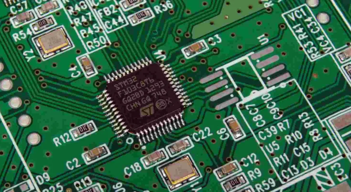
12. Silkscreen Printing
The PCB silkscreen or legend layer is printed after solder mask and surface finishing.
It can contain:
- Component reference designators
- Polarity indicators
- Product information
- Company logos
- Warning symbols
- Assembly instructions
Silkscreen information helps engineers and technicians identify components and simplify PCB assembly, testing, maintenance, and repair.
13. PCB Electrical Testing and Inspection
Before shipment, finished PCBs undergo comprehensive quality inspection and electrical testing.
Depending on the product requirements, testing may include:
- AOI inspection
- Flying probe testing
- Electrical continuity testing
- Short-circuit testing
- Insulation resistance testing
- High-voltage testing
- X-ray inspection
- Dimensional inspection
- Impedance testing
- Microsection analysis
- Visual inspection
Electrical testing verifies that the PCB does not contain unintended open circuits or short circuits.
For high-density and high-reliability PCBs, additional inspection methods may be required to verify internal structures and plated-hole quality.
14. PCB Routing, V-Cut, and Board Separation
After inspection, PCB panels are separated into individual boards or prepared for the customer’s assembly process.
Common methods include:
- CNC routing
- V-scoring / V-cut
- Punching
The appropriate separation method depends on PCB geometry, material, thickness, tolerances, and assembly requirements.
15. Final Inspection and Packaging
After all manufacturing and testing processes are completed, the finished PCBs undergo a final quality inspection.
The manufacturer verifies the boards against the customer’s specifications, including:
- Board dimensions and dimensional tolerances
- Layer count and stack-up accuracy
- Surface finish quality and reliability
- Copper thickness consistency
- Solder mask coverage and quality
- Silkscreen clarity and accuracy
- Hole size, location, and drilling precision
- Electrical performance and functional testing
- Cosmetic appearance requirements
Qualified PCB boards are then carefully packaged using appropriate protective materials to prevent moisture absorption, contamination, oxidation, and physical damage during storage and transportation.
Proper packaging is an essential part of the PCB manufacturing process, as it helps maintain the quality and reliability of finished circuit boards before they are delivered to customers.
Common PCB packaging methods include vacuum packaging with moisture barrier bags, desiccant protection, and anti-static packaging materials to ensure that the boards remain in optimal condition throughout the supply chain.
Why Process Control Is Critical in PCB Manufacturing
Every stage of the PCB manufacturing process directly affects the final product’s performance, reliability, and service life.
Even minor process deviations during PCB fabrication can result in serious quality issues.
For example:
- Poor inner-layer etching may cause open circuits or short circuits, affecting electrical connectivity.
- Improper lamination processes may lead to delamination, layer shifting, or reliability failures.
- Insufficient hole metallization can result in poor electrical connections and via failures.
- Inadequate copper plating thickness may reduce the reliability of vias and plated through holes (PTH).
- Poor solder mask alignment may negatively affect PCB assembly quality and soldering performance.
- Improper surface finishing processes may reduce solderability, corrosion resistance, and long-term PCB reliability.
Therefore, a professional PCB manufacturer requires more than advanced manufacturing equipment. It also requires:
- Strict process control systems
- Experienced PCB engineering teams
- High-quality raw materials
- Advanced manufacturing technologies
- Comprehensive quality inspection procedures
A reliable PCB fabrication supplier must maintain consistent production standards throughout every manufacturing stage to ensure stable quality and high product reliability.
PCB Manufacturing: From Design Data to Finished Circuit Boards
The PCB manufacturing process is a complex combination of chemical processing, mechanical machining, precision imaging, copper plating, thermal processing, inspection, and electrical testing.
From initial design data verification to final product delivery, every step requires accurate control and professional engineering management.
The simplified PCB fabrication workflow can be summarized as:
PCB Design → Inner Layer Fabrication → AOI Inspection → Lamination → Drilling → Hole Metallization → Outer Layer Fabrication → Solder Mask Application → Surface Finish → Silkscreen Printing → Electrical Testing → Final Inspection → Packaging
For electronic manufacturers, engineers, and procurement teams, understanding the complete PCB manufacturing process makes it easier to:
- Evaluate PCB suppliers
- Communicate technical requirements effectively
- Identify potential manufacturing risks
- Select suitable PCB manufacturing solutions
- Improve product reliability and production efficiency
With professional engineering support, strict quality management systems, and optimized production capabilities, Kingda provides reliable PCB manufacturing solutions for customers worldwide.
Through advanced fabrication technologies and comprehensive quality control, Kingda supports the development and production of high-performance printed circuit boards for a wide range of applications, including consumer electronics, industrial equipment, automotive electronics, communication systems, medical devices, and other advanced electronic products.