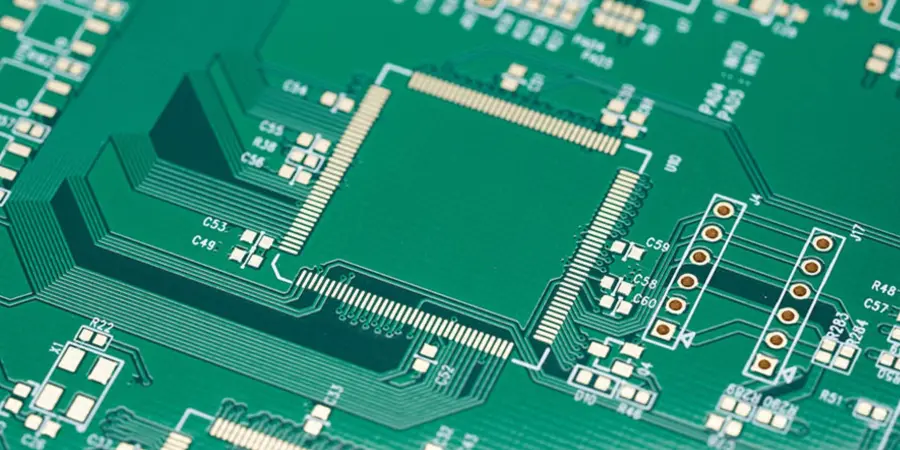
148-Point PCB Design Checklist for Reliable PCB Development
A reliable printed circuit board requires more than a correct schematic and completed routing. Every stage, from initial design data and component placement to signal integrity, EMC, power distribution, manufacturing documentation, and final file verification, should be carefully reviewed before production.
This comprehensive PCB Design Checklist provides 148 inspection items covering the complete PCB design and manufacturing preparation process. It can be used by hardware engineers, PCB designers, engineering teams, and manufacturers as a practical reference before releasing a board for fabrication and assembly.
1. Design Data Input Stage
Before starting layout work, all design information should be complete, accurate, and consistent with the project requirements.
Design Documentation and Template Checks

1. Confirm that all required design documents have been received, including the schematic, *.brd file, BOM, PCB design specifications, PCB design or modification requirements, standardization requirements, and process design documentation.
2. Confirm that the latest PCB template is being used.
3. Verify that the positioning and locating features in the PCB template are correct.
4. Confirm that the PCB design specifications, PCB design or modification requirements, standardization requirements, and related technical instructions are clearly defined.
5. Confirm that component placement restrictions and routing keep-out areas shown in the mechanical drawing have been correctly reflected in the PCB template.
6. Compare the mechanical drawing with the PCB design and verify that all dimensions and tolerances are correct. Confirm that plated and non-plated holes are accurately defined.
7. After confirming that the PCB template is correct, lock the structural file whenever possible to prevent accidental movement or modification.
2. Post-Layout Inspection Stage
After component placement has been completed, perform a comprehensive review before beginning or finalizing routing.
a. Component Inspection
8. Confirm that all component footprints are consistent with the company’s approved library and that the latest footprint library has been used. Review the library update results and update symbols when inconsistencies are found.
9. For motherboards and daughterboards, or single boards and backplanes, confirm signal correspondence, component positions, connector orientation, and silkscreen identification. Verify that daughterboards include anti-mating or incorrect-insertion protection and that components on the daughterboard do not interfere with the motherboard.
10. Confirm that 100% of the required components have been placed.
11. Enable the placement boundaries for both TOP and BOTTOM layers and check whether any overlapping components create acceptable or unacceptable DRC violations.
12. Confirm that there are sufficient and necessary fiducial marks.
13. Heavy components should be positioned close to PCB support points or support edges to reduce PCB warpage.
14. Components related to mechanical structures should preferably be locked after placement to prevent accidental movement.
15. Within 5 mm around press-fit connectors, no component higher than the connector height should be placed on the front side. No components or solder joints should be placed on the back side within the specified area.
16. Confirm that component placement meets manufacturing requirements, with particular attention to BGA, PLCC, and SMT connectors.
17. Pay special attention to metal-housed components and ensure sufficient clearance between them and other components.
18. Components associated with interfaces should be placed as close as practical to their corresponding interfaces. Backplane bus drivers should be positioned close to backplane connectors whenever possible.
19. Confirm that CHIP components located on the wave-soldering side have been converted to appropriate wave-soldering footprints.
20. Confirm whether the number of manual soldering points exceeds 50.
21. For tall axial through-hole components, consider horizontal installation. Reserve sufficient space for horizontal placement and consider the required mechanical fixing method, such as retaining pads for crystals.
22. For components requiring heat sinks, confirm that sufficient clearance exists from surrounding components and verify the height of components within the heat-sink area.
b. Functional Inspection
23. For mixed-signal boards, verify that digital and analog components are properly separated and that the signal flow is logical.
24. Place A/D converters appropriately across the analog/digital partition.
25. Confirm that clock-related components are positioned appropriately.
26. Confirm that high-speed signal components are positioned appropriately.
27. Confirm that termination components are correctly positioned. Source termination resistors should be located near the signal driver, intermediate termination resistors should be positioned at the appropriate midpoint, and terminal termination resistors should be located near the signal receiver.
28. Confirm that the quantity and placement of IC decoupling capacitors are appropriate.
29. When signal traces use planes at different voltage levels as reference planes and cross plane-split areas, confirm that the connecting or decoupling capacitors between the reference planes are located close to the relevant signal routing area.
30. Confirm that protection circuits are positioned appropriately and that their layout facilitates proper partitioning.
31. Confirm that the fuse for the single-board power supply is located close to the connector and that no circuit components are placed before the fuse.
32. Confirm that strong and weak signal circuits, where the power difference is approximately 30 dB, are routed separately.
33. Follow applicable design guidelines and proven design practices for components that may affect EMC testing. For example, the reset circuit on a front panel should be positioned relatively close to the reset button.
c. Thermal Inspection
34. Thermally sensitive components, including liquid-electrolyte capacitors and crystal oscillators, should be positioned away from high-power components, heat sinks, and other heat sources whenever possible.
35. Confirm that the layout meets thermal design requirements and that appropriate thermal paths have been provided according to the process design documentation.
d. Power Supply Inspection
36. Confirm that IC power supply components are not located too far from the corresponding IC.
37. Verify that the LDO and surrounding circuits are laid out appropriately.
38. Verify that module power supply circuits and their surrounding components are laid out appropriately.
39. Confirm that the overall power distribution and placement are reasonable.
e. Design Rule Configuration
40. Confirm that all simulation constraints have been correctly added to the Constraint Manager.
41. Confirm that physical and electrical rules have been correctly configured, paying particular attention to power and ground network constraints.
42. Confirm that the spacing rules for Test Vias and Test Pins are sufficient.
43. Confirm that the PCB stack-up thickness and structure meet both design and manufacturing requirements.
44. For all differential pairs requiring controlled impedance, confirm that impedance has been calculated and that the corresponding design rules have been applied.
3. Post-Routing Inspection Stage
After routing is completed, perform a detailed inspection of signal integrity, power distribution, EMC, reliability, manufacturing constraints, and documentation.
f. Digital and Analog Routing
45. Confirm that digital and analog traces are separated appropriately and that the overall signal flow remains logical.
46. For A/D, D/A, and similar circuits using divided ground areas, verify whether signals between the two areas are routed through the bridge point between the grounds, except where differential signaling is used.
47. Signals that must cross a gap between split power planes should reference a continuous ground plane.
48. If a ground-layer zoning strategy is used without physically splitting the ground plane, ensure that digital and analog signals are routed within their respective functional zones.
g. Clock and High-Speed Signals
49. Confirm that the impedance of high-speed signal traces remains consistent across different PCB layers.
50. Confirm that high-speed differential pairs and similar high-speed signals meet length-matching and symmetry requirements and are routed close to and in parallel with the appropriate reference path.
51. Clock traces should preferably be routed on internal layers.
52. Confirm that clock traces, high-speed signals, reset signals, and other strongly radiating or sensitive signals follow the 3W routing principle whenever applicable.
53. Confirm that clock signals, interrupt signals, reset signals, 100 Mbps/1 Gbps Ethernet signals, and other high-speed signals do not contain unnecessary branch test points.
54. Confirm that low-level signals such as LVDS maintain an appropriate separation from TTL/CMOS signals, preferably following the 10H principle, where H represents the distance between the signal trace and its reference plane.
55. Confirm that clock and high-speed traces avoid densely populated via areas and routing between component pins whenever possible.
56. Confirm that clock routing meets signal-integrity requirements. Clock traces should use as few vias as practical, remain short, and maintain a continuous reference plane, preferably GND. When changing layers and changing the main GND reference layer, provide GND vias within approximately 200 mil of the signal via. When changing between different voltage reference planes, provide appropriate decoupling capacitors within approximately 200 mil of the transition.
57. Confirm that differential pairs, high-speed signal traces, and various buses satisfy the applicable signal-integrity constraints.
h. EMC and Reliability
58. For crystal oscillators, confirm that a ground layer is provided beneath the device and that signal traces do not pass between its pins. Apply the same principle to high-speed sensitive components.
59. Avoid sharp angles and 90-degree corners on signal traces. Continuous 135-degree routing is generally preferred. RF traces should preferably use curved routing or calculated corner structures where appropriate.
60. For double-sided boards, confirm that high-speed signal traces are routed close to their return ground paths. For multilayer boards, ensure that high-speed traces are routed as close as practical to the ground plane.
61. For signal traces on adjacent layers, use perpendicular routing whenever practical to reduce coupling.
62. Avoid routing signal traces underneath power modules, common-mode inductors, transformers, filters, and similar noise-sensitive components whenever possible.
63. Avoid long-distance parallel routing of high-speed signals on the same layer whenever possible.
64. Check whether shielding vias are provided around the divided edges of digital ground, analog ground, and protective ground near the PCB edge. Confirm that multiple ground planes are properly connected with vias. Via spacing should be sufficiently small for the highest-frequency signal, with the source checklist recommending less than one-twentieth of the corresponding wavelength.
65. Confirm that signal traces connected to surge-suppression components are short and wide on the surface layer.
66. Confirm that power and ground planes contain no isolated islands, excessive slots, long cracks caused by large thermal clearances or dense through-via structures, narrow strips, or excessively restricted current paths.
67. Where signal traces change layers frequently, provide ground vias as required. At least two ground planes should be appropriately connected.
i. Power and Ground
68. If power or ground planes are divided, avoid routing high-speed signals across the resulting reference-plane gaps whenever possible.
69. Confirm that power and ground structures can carry the required current. Verify that the number of vias is sufficient for the expected current. As a reference, with 1 oz copper on an outer layer, approximately 1 A/mm of trace width may be used as an estimation, while 0.5 A/mm may be used for inner layers. Short traces may support approximately twice the current under suitable conditions.
70. For power supplies with special requirements, confirm that voltage-drop requirements are satisfied.
71. To reduce plane-edge radiation, attempt to follow the 20H principle between the power and ground layers. Where design conditions permit, a greater power-plane setback can provide additional benefit.
72. If the ground plane is divided, confirm that the divided ground sections do not create unintended current loops.
73. Avoid overlapping adjacent power planes at different voltage levels.
74. Confirm that the isolation between protective ground, -48 V ground, and GND is greater than 2 mm where required.
75. Confirm that -48 V ground is used only as the -48 V signal return path and is not connected to other ground systems. If this cannot be achieved, document the reason in the design notes.
76. Near connector-panel areas, consider providing a 10–20 mm protective-ground region and connecting the relevant layers using staggered rows of vias.
77. Confirm that the spacing between power traces and other signal traces meets applicable electrical safety requirements.
j. Keep-Out Areas
78. Beneath metal-housed components and heat sinks, do not place traces, copper areas, or vias that could potentially cause a short circuit.
79. Around mounting screws and washers, ensure that traces, copper areas, and vias cannot cause short circuits.
80. Confirm that reserved areas specified by the mechanical or design requirements contain no unintended routing.
81. For non-plated holes, maintain an inner-layer clearance greater than 0.5 mm (20 mil) from traces and copper, and an outer-layer clearance greater than 0.3 mm (12 mil). For single-board extraction-tool holes, the recommended inner-layer clearance from traces and copper is greater than 2 mm (80 mil).
82. The recommended clearance between copper areas or traces and the PCB edge is greater than 2 mm, with 0.5 mm as the minimum reference value.
83. For inner-layer ground copper, maintain approximately 1–2 mm clearance from the PCB edge, with 0.5 mm as the minimum reference value.
k. Pad Routing
84. For two-pad CHIP components such as 0805 and smaller resistors and capacitors, traces should preferably exit symmetrically from the center region of the pads. The traces connected to both pads should have the same width. This requirement may be relaxed for traces narrower than 0.3 mm (12 mil).
85. For pads connected to wider traces, use a short narrower trace section as a transition whenever appropriate, particularly for 0805 and smaller components.
86. For SOIC, PLCC, QFP, SOT, and similar packages, route traces from the two ends of the pads whenever practical.
l. Silkscreen
87. Confirm that no component reference designators are missing and that their positions allow the corresponding components to be correctly identified.
88. Confirm that all component reference designators comply with the applicable company or project standards.
89. Verify component pin numbering, Pin 1 indicators, component polarity markings, and connector orientation indicators.
90. Confirm that the insertion direction markings between motherboards and daughterboards correspond correctly.
91. Confirm that backplanes correctly identify slot names, slot numbers, port names, and connector orientation.
92. Confirm that all required silkscreen information has been added correctly.
93. Confirm that electrostatic-discharge and RF board identification markings have been added where required.
m. PCB Identification and Barcodes
94. Confirm that the PCB identification code is correct and complies with applicable specifications.
95. Confirm that the PCB identification code is located on the correct side and layer. The source checklist specifies the upper-left area of the A-side silkscreen as the recommended location.
96. For backplanes, confirm that the PCB identification code is located on the correct side and layer. The source checklist specifies the upper-right area of the B-side outer copper layer.
97. Confirm that a white silkscreen area is reserved for barcode laser marking.
98. Confirm that no traces or conductive vias larger than 0.5 mm are located beneath the barcode area.
99. Confirm that no components higher than 25 mm are located within 20 mm outside the white barcode silkscreen area.
n. Vias
100. On the reflow-soldering side, vias should not normally be placed directly on pads. For exposed vias, the recommended clearance from pads is greater than 0.5 mm (20 mil). For solder-mask-covered vias, the recommended clearance from pads is greater than 0.1 mm (4 mil). Use the appropriate Same Net DRC settings to verify these requirements.
101. Avoid excessively dense via arrangements that may cause large-scale interruptions in power or ground planes.
102. The recommended via hole diameter should generally not be smaller than one-tenth of the PCB thickness.
o. Manufacturing Process
103. Confirm that component placement coverage is 100% and routing completion is 100%. Any area that cannot reach 100% should be documented in the design notes.
104. Reduce dangling traces as much as possible. Any remaining dangling traces should be individually reviewed and confirmed.
105. Carefully review and verify all manufacturing issues identified by the process engineering team.
p. Large Copper Areas
106. For large copper areas on the TOP and BOTTOM layers, use grid copper when there is no special requirement. For single boards, diagonal grids may be used; for backplanes, orthogonal grids may be used. A reference configuration is 0.3 mm (12 mil) line width with 0.5 mm (20 mil) spacing.
107. Component pads within large copper areas should preferably use thermal-relief connections to reduce the risk of insufficient soldering. When higher current capacity is required, first consider widening the thermal spokes before using a fully connected copper configuration.
108. When applying large copper areas, avoid unconnected dead copper or isolated copper islands whenever possible.
109. Check large copper areas for illegal connections and any unreported DRC violations.
q. Test Points
110. Confirm that sufficient test points are provided for power and ground networks. As a reference, at least one test point may be provided for every 2 A of current.
111. Confirm that all networks without test points have been reviewed and verified as suitable for test-point reduction or omission.
112. Confirm that test points are not assigned to components that will not be installed during production.
113. Confirm that Test Vias and Test Pins are fixed where required, especially for design modifications using an unchanged test fixture.
r. DRC
114. Set the spacing rules for Test Vias and Test Pins to the recommended values first. Run DRC and, if violations remain, perform another check using the minimum permitted spacing.
115. Enable the appropriate design constraints, update the DRC results, and review all remaining violations to determine whether any prohibited errors exist.
116. Reduce DRC violations to the minimum possible level. Every violation that cannot be eliminated must be individually reviewed and confirmed.
s. Optical Fiducial Marks
117. Confirm that each PCB side containing SMT components has appropriate optical fiducial marks.
118. Confirm that optical fiducial marks do not overlap traces or silkscreen elements.
119. The background surrounding optical fiducials should remain consistent. For board-level fiducials, confirm that the center of each fiducial is at least 5 mm from the PCB edge.
120. Confirm that board-level optical fiducial reference marks have assigned coordinates. It is recommended to place fiducials as component objects and use integer coordinate values in millimeters.
121. For ICs with pin pitch below 0.5 mm and BGAs with pin pitch below 0.8 mm (31 mil), provide optical fiducial marks near the diagonal areas of the component.
t. Solder Mask Inspection
122. Confirm that all pads requiring special treatment have been correctly opened in the solder mask, with particular attention to hardware design requirements.
123. Confirm that vias beneath BGA components have been properly processed as solder-mask-covered or plugged vias where required.
124. Except for test vias, confirm that other vias have been appropriately processed with small openings or solder-mask coverage/plugging according to the manufacturing requirements.
125. Confirm that solder-mask openings around optical fiducial marks do not expose unintended copper or traces.
126. For power-management ICs, crystal oscillators, and other components requiring copper for thermal dissipation or grounding/shielding, confirm that the copper area is correctly provided and that the solder mask is properly opened. Components secured by solder should include appropriate solder-mask barriers to prevent excessive solder spreading.
4. Manufacturing File Preparation
After the PCB layout has passed design inspection, manufacturing documentation must be checked carefully before release.
u. Drill Drawing
127. Confirm that the drill drawing notes correctly specify PCB thickness, layer count, silkscreen color, warpage requirements, and other technical requirements.
128. Confirm that layer names, layer order, dielectric thickness, and copper thickness in the stack-up drawing are correct. If controlled impedance is required, verify that the description is accurate. Confirm that stack-up layer names correspond correctly to the associated Gerber filenames.
129. Disable the Repeat Code option in the appropriate setup table and set the drilling precision to the required range, with the source checklist specifying 2–5.
130. Confirm that the hole table and drill files are up to date. Whenever holes are modified, regenerate the corresponding files.
131. Check the hole table for abnormal hole sizes. Confirm that holes for press-fit components are correctly defined and that hole tolerances are properly specified.
132. Vias requiring plugging should be listed separately and clearly identified as “filled vias.”
v. Gerber Files
133. Whenever possible, output Gerber files using the RS-274X format with a recommended precision of 5:5.
134. Confirm that the art_aper.txt file is up to date when required. It may not be necessary when using the RS-274X format.
135. Review the Gerber output log and confirm that there are no abnormal warnings or errors.
136. Check the edges and isolated areas of negative layers carefully.
137. Use a Gerber inspection tool to verify that the Gerber files match the PCB design. For modified boards, use a comparison tool to identify differences from the previous revision.
5. Complete Manufacturing Documentation Package
A complete production package should contain all required design, manufacturing, assembly, structural, testing, and archival documents.
138. PCB design file:
Product Model_Specification_Board Code_Revision.brd
139. Backplane support-board design file:
Product Model_Specification_Board Code_Revision-CB[-T/B].brd
140. PCB manufacturing package:
PCB Code.zip
The package should include Gerber files for each layer, aperture files, drill files, and ncdrill.log. Panelized boards should also include the process-provided panelization file (*.dxf). Backplanes should additionally include the support-board package:
PCB Code-CB[-T/B].zip
This package should include files such as drill.art, *.drl, and ncdrill.log.
141. Process design document:
Product Model_Specification_Board Code_Revision-GY.doc
142. SMT coordinate file:
Product Model_Specification_Board Code_Revision-SMT.txt
When exporting the coordinate file, confirm that Body Center is selected. Symbol Origin should only be selected when all SMD component libraries have their origins correctly defined at the component center.
143. PCB mechanical structure file:
Product Model_Specification_Board Code_Revision-MCAD.zip
The package should contain the DXF and EMN files supplied by the mechanical/structural engineering team.
144. Test file package:
Product Model_Specification_Board Code_Revision-TEST.ZIP
The package should include testprep.log and untest.lst or the coordinate file for test points.
145. Archived drawing file:
Product Model_Specification_Board Name_Revision.pdf
The archived drawing should include the cover page, first page, silkscreen layers, routing layers, drill drawing, and, where applicable, the backplane support-board drawing.
6. Standardization
The final stage is to verify that all drawings and documentation comply with the applicable project and company standards.
146. Confirm that all information on the cover page and first page is correct.
147. Confirm that drawing numbers are correct and correspond to the appropriate PCB layer sequence.
148. Confirm that the PCB identification code shown in the drawing title block is correct.
Why a Complete PCB Design Checklist Matters
A structured PCB Design review helps identify problems before they become manufacturing or assembly issues. Component placement, signal integrity, grounding, power distribution, EMC, thermal management, DRC, manufacturing documentation, and testing requirements are closely interconnected.
For complex electronic products, a design that passes basic electrical verification may still encounter manufacturing, assembly, or reliability problems. A comprehensive review therefore needs to consider both electrical functionality and manufacturability.
Professional DFM Analysis can identify potential manufacturing risks before fabrication, including insufficient spacing, unsuitable drill structures, component clearance issues, stack-up problems, and other production constraints.
GOPCBA provides PCB design support covering stack-up design, impedance calculation, PCB layout, EMC inspection, and manufacturability evaluation. Its published PCB design capabilities support complex high-speed, high-density, multilayer, HDI, and controlled-impedance projects.
For projects moving from design into production, professional PCB Manufacturing should also include engineering review, material selection, fabrication process control, electrical testing, and final inspection. GOPCBA’s manufacturing capabilities cover multilayer, HDI, high-frequency, rigid-flex, heavy-copper, metal-core, and controlled-impedance PCB technologies.
Quality control should continue throughout fabrication and assembly. A structured quality system can include pre-production checks, PCB specification verification, BOM review, manufacturing process controls, incoming inspection, electrical testing, and final inspection.
For projects requiring integrated production, PCB Assembly can combine PCB fabrication, component procurement, SMT/THT assembly, inspection, testing, and final integration into a coordinated manufacturing workflow.
If your project requires professional PCB engineering, fabrication, assembly, or manufacturing support, you can contact GOPCBA for project evaluation and technical assistance.