Why Do PCB Prototypes Keep Failing? 5 Critical Details You Should Never Overlook
PCB prototyping is an essential step for validating an electronic product before moving into larger-scale production. A well-made prototype can reveal design issues, manufacturing risks, assembly problems, and performance limitations before they become expensive production failures.
However, many PCB projects still experience repeated prototype failures. The finished board may not meet the required specifications, fail functional testing, or even become unusable. These problems can increase development costs and delay product launches.
In many cases, prototype failure is not caused by an extremely complicated technical problem. Instead, it often comes from small details that were overlooked during specification, material selection, manufacturing, testing, or communication.
Here are five critical areas that deserve particular attention.
1. Unclear Requirements Can Lead to the Wrong PCB Prototype
The first step in successful PCB prototyping is making sure the manufacturer fully understands the project requirements.
Unfortunately, specifications are sometimes communicated using vague descriptions such as “high temperature resistant,” “high reliability,” or “durable surface finish.” These descriptions may not provide enough technical information for a manufacturer to make the correct production decisions.
For example, a high-temperature application should specify the expected operating temperature and exposure duration. Similarly, a project requiring durable electrical contacts may need a particular surface finish based on the number of mating cycles and environmental conditions.
Other important specifications can include:
- Board dimensions and thickness
- Number of PCB layers
- Copper thickness
- Minimum trace width and spacing
- Hole and via specifications
- Material requirements
- Surface finish
- Impedance requirements
- Operating temperature
- Electrical testing requirements
- Mechanical and environmental requirements
Before production begins, prepare a clear and written specification document. If certain requirements are uncertain, ask your PCB manufacturer for engineering recommendations and confirm the final decision in writing.
For customers who need support beyond fabrication, PCB Design & Layout services can help identify potential design and manufacturability issues before the prototype enters production.
2. Incorrect Material Selection Can Cause Prototype Failure
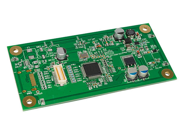
PCB materials directly affect electrical performance, thermal stability, mechanical reliability, and manufacturing results.
Choosing an unsuitable material is therefore one of the most common causes of prototype problems.
For example, a standard FR-4 material may not be the best choice for applications requiring particularly high thermal performance. Likewise, copper thickness must be selected according to current-carrying requirements. Using copper that is too thin may create electrical or thermal problems, while excessive copper thickness can affect manufacturing tolerances and routing space.
Surface finish also needs to match the application’s requirements. Different finishes provide different characteristics in terms of solderability, corrosion resistance, electrical performance, cost, and contact durability.
Before manufacturing, review at least the following:
- Base material and material grade
- Tg and thermal performance
- Dielectric properties
- Copper thickness
- Board thickness
- Surface finish
- Solder mask requirements
- Via and hole construction
- Environmental requirements
A capable PCB supplier should be able to review these requirements and identify potential material-selection risks before fabrication begins.
For more complex projects, manufacturers offering PCB Manufacturing capabilities across multilayer, HDI, high-frequency, rigid-flex, and heavy-copper technologies can provide more options when selecting the appropriate construction.
3. Poor Coordination Between Manufacturing Processes Can Multiply Small Errors
A PCB prototype usually involves multiple manufacturing and assembly processes. These may include material preparation, inner-layer fabrication, lamination, drilling, plating, imaging, etching, surface finishing, component placement, soldering, and inspection.
When information is not transferred correctly between processes, a small problem can become a major production failure.
For example, an incorrect board dimension may affect drilling and component placement. A substrate defect discovered during assembly may become much more expensive to correct if production continues without intervention. Likewise, surface-finish problems that are not detected early can affect solderability and final reliability.
A better approach is to establish clear process handoffs and inspection checkpoints.
At each important stage, production teams should verify:
- Dimensional accuracy
- Layer alignment
- Hole position and quality
- Trace geometry
- Surface condition
- Solderability
- Assembly quality
- Electrical continuity
- Manufacturing deviations
Any abnormal condition should be reported and evaluated before the board moves to the next process.
This is particularly important when prototype fabrication and assembly are handled as separate services. A coordinated PCB Assembly process can help connect PCB fabrication, component sourcing, SMT, through-hole assembly, inspection, and testing into a more controlled workflow.
4. Skipping Testing Removes the Last Opportunity to Catch Problems
A prototype exists to validate the product—not simply to produce a physical board.
For this reason, testing should not be treated as optional simply because the prototype quantity is small.
Checking only whether a circuit has electrical continuity may not be sufficient. Depending on the application, additional verification may be required for insulation, solder joints, mechanical characteristics, signal performance, thermal behavior, or environmental reliability.
A practical prototype verification plan may include:
Electrical Testing
Electrical testing can help identify open circuits, short circuits, incorrect connections, and other manufacturing defects.
Visual and Automated Inspection
Visual inspection and automated inspection can identify soldering problems, component placement issues, PCB surface defects, and other visible abnormalities.
Functional Testing
Functional testing verifies whether the assembled PCB actually performs according to the product’s intended operating requirements.
Environmental Testing
For products exposed to demanding conditions, testing may include temperature, humidity, vibration, or other environmental conditions appropriate to the application.
The exact testing strategy should be determined by the PCB’s design, application, risk level, and customer requirements.
For projects requiring a stronger validation process, Prototype PCB Assembly can help bridge the gap between PCB design verification and assembled prototype evaluation.
5. Delayed Communication Can Turn a Fixable Issue Into a Failed Prototype
Even with good engineering and manufacturing processes, unexpected issues can occur during prototyping.
The critical question is how quickly those issues are identified and communicated.
Suppose a manufacturer discovers that the specified layer count and board thickness create a manufacturing conflict. If the issue is not communicated promptly, the manufacturer may make assumptions and continue production. The resulting prototype may then fail to meet the original design requirements.
The same problem can occur when a customer changes:
- PCB material
- Surface finish
- Component selection
- Board thickness
- Electrical requirements
- Mechanical dimensions
- Delivery requirements
Any change should be communicated as early as possible so its impact on manufacturing, cost, and lead time can be evaluated.
A good PCB supplier should not simply manufacture according to the original files without question. When an obvious engineering conflict or manufacturing risk is identified, proactive communication can prevent unnecessary rework.
How to Improve PCB Prototype Success Rates
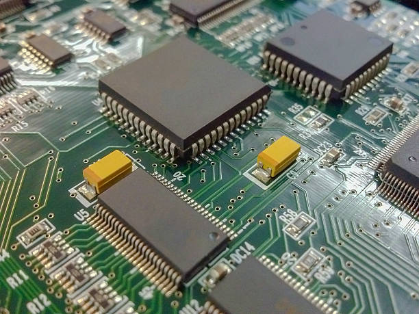
Successful PCB prototyping requires more than simply uploading Gerber files and waiting for finished boards.
A reliable process should connect design, materials, manufacturing, assembly, inspection, testing, and communication.
Before submitting a prototype order, consider using the following checklist:
- Confirm all PCB specifications in writing.
- Verify material type, copper thickness, and surface finish.
- Review the design for manufacturability.
- Confirm manufacturing tolerances and special processes.
- Establish inspection and testing requirements.
- Make sure PCB fabrication and assembly requirements are consistent.
- Communicate design changes immediately.
- Review prototype results before moving into mass production.
For projects that require small quantities for engineering validation, Low Volume PCB Assembly can provide a practical bridge between prototype development and larger-scale production.
Conclusion
Repeated PCB prototype failures are rarely just a matter of bad luck. In many cases, the root cause can be traced back to unclear specifications, incorrect materials, manufacturing coordination problems, insufficient testing, or delayed communication.
The key is to treat prototyping as an engineering validation process rather than simply a small production order.
By clearly defining requirements, selecting appropriate materials, coordinating manufacturing and assembly, implementing suitable testing, and maintaining fast communication with your manufacturing partner, you can significantly reduce prototype failures, shorten development cycles, and create a more reliable path toward mass production.
Choosing an experienced PCB supplier that can support design review, PCB manufacturing, assembly, testing, and production scale-up can make the entire development process more predictable and efficient.