Radar System High-Frequency PCB Manufacturing
Radar hardware turns weak echoes into usable target data, and the PCB carries every one of those signals. At microwave and millimeter-wave frequencies, small process drift becomes large yield loss. A board that behaves well at low frequency can fail once the same design runs at radar bands. Manufacturing decisions therefore start earlier and are checked harder than on ordinary digital boards. This article explains what buyers and engineers should verify before releasing a radar high-frequency build.
The work splits into four connected areas: material choice, stackup and impedance control, fabrication precision, and test coverage. Each area feeds the next, so a weak choice in one place shows up as a measurement failure somewhere else. A supplier who understands this chain can flag risk during file review rather than after lamination. A buyer who understands it can compare quotations on evidence instead of headline price. The sections below follow that order from material to final test.
Radar Signal Path Requirements
Radar circuits operate at frequencies where transmission loss grows quickly with distance and dielectric quality. The board must carry RF energy with low attenuation and stable phase behavior across the band of interest. It must also separate sensitive receive paths from noisy digital and power sections. Every routing decision, layer assignment, and copper feature affects that balance. Requirements should be written down before layout starts, because late changes to a high-frequency stackup are expensive and slow.
Impedance control is the second fixed requirement. Variations in trace width, dielectric thickness, copper thickness, or layer registration shift impedance away from target. Those shifts cause reflections and insertion loss, especially on long RF runs. Impedance targets belong in the fabrication drawing, not only in the design file. The supplier should confirm which structures will be measured and how tolerance will be reported. Without that agreement, a passing board and a failing system can come from the same lot.
Material Selection Tradeoffs
Low-loss dielectric materials sit at the center of radar board performance. PTFE-based laminates and similar low-loss systems suit demanding RF paths, while conventional FR-4 remains workable for control and power layers. The right choice depends on operating frequency, dielectric constant, dissipation factor, thermal limits, and mechanical needs. Cost and production volume also matter, because specialty materials carry longer lead times. Engineers should match material to the actual band rather than defaulting to the most expensive option.
Hybrid stackups combine high-frequency material on RF layers with FR-4 on digital and power layers. This approach can balance electrical performance against cost and mechanical behavior. It also adds process risk, because dissimilar materials expand and press differently during lamination. The supplier must control bake, bonding, and cure for each material system. Buyers should ask how hybrid builds are qualified and which prepregs are approved. A stackup that looks efficient on paper can create delamination or thickness variation if the press cycle is not tuned.
Stackup and Impedance Planning
Stackup planning links electrical intent to physical construction. Layer count, dielectric thickness, copper weight, and reference plane placement all set the impedance environment. RF traces need continuous reference planes and short return paths. Sensitive receive lines should stay away from switching supplies and fast digital edges. Ground stitching and via placement complete the return path at transitions. These choices are cheaper to fix in layout than in fabrication, so review them early with the board shop.
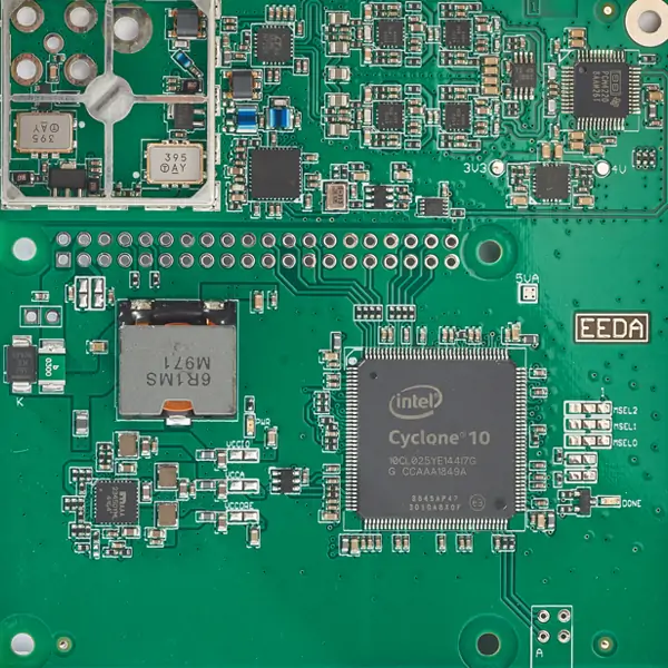
Impedance verification closes the loop between design and production. Coupon structures built beside the panel allow the shop to measure actual impedance after lamination. Results should be recorded against the lot and shared with the customer. If measured values drift, the cause may be etch bias, prepreg flow, or plating thickness. Finding that cause quickly protects the next build. A clear PCB design and layout review before tooling helps align these numbers from the start.
Precision Fabrication Steps
Fine-line imaging and controlled etching keep conductor geometry close to the design. On RF boards, small changes in trace width shift impedance and loss. Imaging, exposure, development, and plating must therefore run inside a narrow window. The shop should know which features are critical and inspect them first. Process capability should be judged against the real drawing, not against a general catalog claim. Buyers can request first-article measurements on critical traces before the full lot runs.
Multilayer lamination controls layer registration, dielectric thickness, and bond strength. Temperature, pressure, heating rate, and cooling all influence the final result. Poor control shows up as layer misalignment, thickness variation, or voids between layers. Hybrid stacks need extra care because each material has its own press profile. Flatness also matters, since warped panels disturb assembly and test. A supplier with documented press recipes and routine coupon checks gives a more predictable result than one that adjusts by feel.
Surface Finish and Assembly Fit
Surface finish affects solderability, contact resistance, and corrosion behavior over the product life. ENIG and immersion silver are common choices for RF and mixed assemblies, and each brings tradeoffs in cost, shelf life, and process compatibility. The finish must suit the components, the assembly process, and the operating environment. Thin or uneven plating can hurt high-frequency loss on exposed traces. Buyers should confirm finish thickness targets and how they are checked. For sourcing checks on those parts, see our component procurement notes.
When assembly is part of the scope, fabrication and placement must be planned together. Solder mask openings, via treatment, and panel handling all affect yield at the placement line. Component choice matters too, since some RF parts are sensitive to moisture and thermal exposure. Coordinating fabrication with turnkey PCB assembly keeps one team responsible for the finished board. It also shortens the feedback loop when a defect appears at test.
Test Coverage and Quality Records
Electrical test on high-frequency boards goes beyond continuity. Impedance coupons, insertion loss checks, and return loss measurements show whether the RF path behaves as designed. Not every lot needs full network analysis, but critical programs should define which parameters are measured and how often. Visual and automated optical inspection catch opens, shorts, mask defects, and registration errors. Reliability testing adds temperature cycling, humidity exposure, and vibration where the application demands it. A structured quality management system keeps these records tied to the lot.
Records matter as much as the measurements. The shop should keep the press program, material batch, operator, and inspection result for each panel group. That record provides the quickest way to find the cause when a field return comes back months later. Buyers should ask for first-article reports and lot data as a routine part of the order. Suppliers who produce these documents easily usually keep them honestly during production. Documentation that appears only on request deserves a closer look.
Supplier Selection and Volume Planning
Supplier evaluation should focus on capability evidence, not brochure claims. Ask whether the shop handles the specific laminate, layer count, and impedance tolerance your design needs. Review how it qualifies hybrid stackups and how it reports measured data. Confirm that incoming material inspection covers dielectric and copper properties. Ask who reviews the files before tooling and how risks are communicated. A supplier that raises questions early is usually safer than one that accepts every file without comment.
New radar designs benefit from a prototype stage before volume commitment. Early samples reveal stackup problems, impedance drift, and assembly issues while changes are still cheap. Once the design is proven, production planning covers panel utilization, material lead time, and test capacity. Buyers moving toward larger builds should discuss high-volume PCB assembly early, so fabrication and placement capacity are reserved together. Component sourcing should also be reviewed, since RF parts often have limited distribution and long lead times.
Clear specifications reduce disputes later. The drawing should state operating frequency, material, layer count, thickness, copper weight, impedance targets, via structure, finish, and environmental requirements. Tolerances should reflect what the product needs, not a default value copied from another job. Every agreed limit should appear in the first-article report. Buyers who treat specification review as part of the purchase, rather than paperwork, get fewer surprises at incoming inspection.
The practical takeaway is simple. Radar high-frequency PCB manufacturing rewards preparation before tooling. Agree the material and stackup, fix the impedance targets in writing, confirm the press and imaging controls, and require measured data with each lot. Keep prototype, production, and test planning in one conversation. A supplier who can show these records and explain each process window is worth more than a lower quote with no evidence behind it.