How to Change PCB Colors in Altium: PCB Design & Layout Visualization Guide
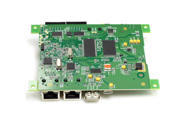
PCB design is the foundation of the final printed circuit board and one of the most critical stages in product development. The PCB layout provides the basis for subsequent PCB manufacturing, assembly, testing, inspection, and troubleshooting.
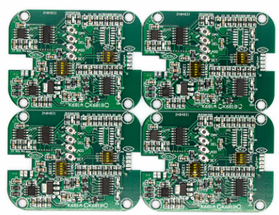
A PCB layout is developed according to the electrical schematic, circuit architecture, engineering requirements, applicable design standards, and the intended application. Professional PCB designers typically use EDA tools such as Altium Designer to place components, route traces, define board layers, create design rules, and prepare manufacturing data.
As PCB designs become more complex, visual organization becomes increasingly important. A multilayer PCB may contain numerous signal layers, power layers, ground planes, vias, pads, components, keepouts, and mechanical features. If all these objects are displayed using similar colors, it can become difficult to interpret the layout efficiently.
This is why many engineers customize the appearance of their PCB designs.
One common question among Altium users is: how to change PCB colors in Altium.
Altium Designer provides several visualization controls that allow users to customize layer colors, system colors, object visibility, layer opacity, network highlighting, and 3D material appearance. Properly configured colors can make complex layouts easier to understand and can significantly improve PCB design efficiency.
This guide explains how to change PCB colors in Altium, including 2D layer colors, 3D PCB colors, individual net colors, visibility settings, and practical color-management recommendations.
Altium PCB Color Settings
Altium Designer provides a centralized visualization environment for controlling how PCB objects appear in the editor.
In the PCB editor, pressing L typically opens the View Configuration panel, where designers can manage layer visibility, colors, display modes, masking, dimming, and other visual settings.
Depending on the Altium Designer version and workspace configuration, the exact names and positions of some controls may differ. However, the general workflow remains similar.
The View Configuration panel can be used to manage:
- PCB layer visibility
- Layer colors
- System colors
- Object display modes
- Dimming and masking
- Transparency
- 3D visualization settings
- Other PCB editor display preferences
Instead of changing the physical properties of the PCB, these settings primarily affect how the design is displayed within the design environment.
This distinction is important: changing a layer’s display color does not change the copper, solder mask, silkscreen, or electrical characteristics of the manufactured PCB.
How to Change PCB Colors in Altium’s 2D Layout
The 2D PCB editor is the primary environment used for component placement, routing, layer management, and design-rule checking.
Step 1: Open the PCB Layout
Open the required PCB document in Altium Designer.
The PCB layout will normally appear in the standard 2D editor view, displaying the board outline, components, copper features, vias, pads, and other design objects.
Step 2: Open View Configuration
Press L to open the View Configuration panel.
You can also access the relevant visualization controls through the PCB editor interface.
The panel provides access to different categories of PCB layers and display settings.
Step 3: Select the Layer
Locate the layer whose display color you want to modify.
Depending on the design, this may include:
- Top Layer
- Bottom Layer
- Internal signal layers
- Internal planes
- Top Solder
- Bottom Solder
- Top Overlay
- Bottom Overlay
- Mechanical layers
- Other user-defined layers
Select the appropriate layer or object category.
Step 4: Change the Layer Color
Use the color control associated with the selected layer to choose a new display color.
For example, designers may use contrasting colors to distinguish:
- Top-layer routing
- Bottom-layer routing
- Power-related structures
- Ground structures
- Mechanical information
- Component outlines
- Silkscreen information
The objective is not simply to make the PCB look attractive. A well-planned color scheme should make the design easier to interpret.
Step 5: Adjust Visibility and Dimming
The View Configuration panel can also be used to hide layers or reduce the visual intensity of inactive layers.
This is particularly useful when working with a dense multilayer PCB.
For example, if you are routing signals on an internal layer, dimming the other layers can make the active routing path much easier to see.
Masking and dimming are especially useful when troubleshooting:
- Dense routing
- Via transitions
- BGA fanout
- Differential pairs
- Power distribution
- Layer-to-layer connections
Saving PCB Color Presets
Once a useful color scheme has been created, Altium allows designers to preserve visualization settings for future use, depending on the software version and configuration.
A customized color scheme can be useful when:
- Working on multiple PCB projects
- Maintaining company design conventions
- Training new PCB designers
- Reviewing multilayer layouts
- Standardizing engineering workflows
If a customized color scheme makes the PCB difficult to interpret, the default visualization settings can be restored.
Maintaining a consistent color convention across projects can reduce the time engineers spend identifying layers and objects.
How to Change PCB Colors in Altium’s 3D Layout
Altium Designer also provides a 3D PCB visualization environment.
The 3D view allows designers to inspect the physical appearance and mechanical relationships of the PCB, including:
- PCB substrate
- Copper structures
- Solder mask
- Silkscreen
- Components
- Connectors
- Mounting holes
- Mechanical features
3D visualization is particularly useful for checking component clearance, enclosure fit, connector orientation, component height, and general mechanical integration.
Opening the 3D View
Switch from the 2D PCB editor to the 3D view using the appropriate Altium command or shortcut.
The exact interface may vary by Altium Designer version, but the 3D visualization controls can generally be accessed through the View Configuration environment.
Changing 3D Material Appearance
Within the 3D visualization settings, users can adjust the appearance of PCB materials and objects.
Depending on the available settings, this may include:
- Board substrate appearance
- Solder mask appearance
- Silkscreen appearance
- Component display
- Transparency
- Lighting
- Surface effects
- Background appearance
For example, changing the solder mask appearance can help designers visualize how the finished PCB may look.
However, it is important to understand that these are primarily visualization settings. The selected display color does not automatically determine the actual solder mask color or surface finish that will be used during PCB manufacturing.
Changing PCB Background and Display Appearance
A suitable background can make PCB objects easier to distinguish.
Altium’s visualization controls allow designers to modify aspects of the workspace appearance, including background and display effects.
A darker background may make certain bright layer colors easier to see, while a lighter background can be useful for documentation, presentations, or screenshots.
When selecting colors, prioritize contrast and readability rather than aesthetics alone.
For example:
- Use strong contrast between active and inactive layers.
- Avoid similar colors for adjacent signal layers.
- Avoid colors that are difficult to distinguish for extended periods.
- Maintain consistent conventions between projects.
- Use dimming to reduce visual clutter.
How to Change the Color of an Individual PCB Net
Sometimes changing the color of an entire PCB layer is not enough.
An engineer may want to highlight a particular network, such as:
- GND
- VCC
- CLK
- RESET
- High-speed differential pairs
- Critical power rails
- Sensitive analog signals
- Important data buses
Altium provides net-color and highlighting functionality that can help designers focus on selected connections.
Step 1: Open the PCB Panel
Open the PCB panel and navigate to the appropriate net-related view.
Depending on the Altium version, the available panel options and terminology may vary.
Step 2: Select the Net
Find the network you want to highlight.
Select one or more nets as required.
Step 3: Assign a Display Color
Use the available net-color or highlighting controls to assign a visual color to the selected network.
The selected net can then be visually distinguished from other routing.
Step 4: Enable the Appropriate Color Override or Highlight Mode
If the selected color does not appear immediately, check the active display or color-override mode.
Refreshing the PCB view may also be necessary depending on the current visualization configuration.
This approach is especially useful for tracing critical connections through dense PCB layouts.
Using Color to Highlight High-Speed PCB Signals
Color customization becomes particularly valuable when working on high-speed PCB design.
High-speed interfaces can contain many closely spaced traces and differential pairs. Highlighting critical nets can make it easier to follow their routing from one component to another.
For example, designers can visually emphasize:
- Differential pairs
- Clock signals
- High-speed serial interfaces
- Memory buses
- Sensitive analog signals
- Power-delivery networks
However, color highlighting should complement—not replace—proper electrical analysis.
Signal integrity still depends on factors such as:
- Controlled impedance
- Trace geometry
- Reference planes
- Return-current paths
- Differential-pair spacing
- Via transitions
- Crosstalk
- Layer transitions
A color scheme improves visualization, but it does not electrically improve a PCB.
Synchronizing PCB and Schematic Visualization
Maintaining consistency between the schematic and PCB layout can make engineering review more efficient.
When a design uses net colors or highlighting conventions, engineers may use available Altium project comparison and synchronization functions to keep design information aligned after engineering changes.
However, color assignments should be treated primarily as visualization metadata rather than as electrical design information.
When transferring engineering changes between schematic and PCB documents, the actual electrical connectivity, component relationships, and design rules remain the critical information.
Best Practices for PCB Color Management
A well-designed color scheme can significantly improve PCB layout readability.
1. Use a Consistent Color Convention
Assign colors systematically.
For example, you may use different colors to distinguish top-layer routing, bottom-layer routing, internal signal layers, power structures, and mechanical information.
The exact colors are less important than consistency.
2. Use Strong Contrast
Avoid assigning similar colors to adjacent layers.
If two layers appear almost identical, it becomes difficult to determine which layer contains a particular trace or via connection.
3. Highlight Critical Nets
Use net highlighting for important signals rather than changing the entire layer color.
This is particularly effective when reviewing:
- Clock networks
- Differential pairs
- Power rails
- Reset signals
- High-speed data paths
4. Dim Inactive Layers
When routing a specific layer, dimming other layers can reduce visual clutter.
This is particularly useful on boards with many copper layers.
5. Avoid Excessive Colors
Using too many colors can make a PCB layout harder to understand rather than easier.
A small number of well-defined colors is generally more effective than assigning a unique color to every object.
6. Consider Color Accessibility
Some color combinations are difficult for people with color-vision deficiencies to distinguish.
Avoid relying exclusively on red/green differences. Combine color with layer names, visibility, object shapes, and other visual cues.
7. Keep Visualization Separate from Manufacturing Specifications
A critical point is that an Altium display color is not necessarily the physical color of the finished PCB.
For example, selecting a particular color for a solder mask layer in Altium does not automatically mean the manufacturer will fabricate the PCB using that solder mask color.
Actual PCB manufacturing specifications must be defined separately in the fabrication documentation and manufacturing data.
Common Mistakes When Changing PCB Colors in Altium
Mistake 1: Confusing Display Color with PCB Manufacturing Color
The color shown in Altium is primarily a visualization property. It should not be used as a substitute for fabrication documentation.
Mistake 2: Using Too Many Similar Colors
Closely related colors can make multilayer routing difficult to distinguish.
Mistake 3: Ignoring Active-Layer Highlighting
When working on a complex layout, failing to configure active-layer and inactive-layer display settings can create unnecessary visual clutter.
Mistake 4: Using Color as the Only Identification Method
Important design information should remain identifiable through layer names, net names, reference designators, design rules, and documentation.
Mistake 5: Forgetting 3D Visualization
A 2D layout may appear correct while mechanical conflicts remain visible only in the 3D environment.
Using both 2D and 3D visualization can provide a more complete understanding of the PCB design.
Why PCB Color Management Matters
Color customization may appear to be a cosmetic feature, but it can improve engineering productivity.
A well-organized visual environment can help designers:
- Identify PCB layers faster
- Trace critical networks
- Review dense routing
- Understand multilayer structures
- Locate potential layout problems
- Inspect component placement
- Communicate design information
- Perform design reviews more efficiently
For complex PCB design, these benefits become increasingly valuable as the number of layers, components, and connections increases.
How Kingda Supports PCB Design and Manufacturing
A successful PCB project requires more than a visually correct layout. The design must also satisfy electrical, mechanical, thermal, and manufacturing requirements.
Kingda can support PCB projects by helping align the manufacturing process with the design requirements defined by the engineering team.
For complex boards, important considerations include:
- PCB layer count
- Material selection
- Copper thickness
- Minimum trace and spacing requirements
- Via structures
- Board thickness
- Controlled impedance
- Surface finish
- Solder mask
- Silkscreen
- Manufacturing tolerances
- Electrical testing
Early communication between the PCB designer and manufacturer can help identify potential DFM issues before fabrication begins.
This is especially important for multilayer, HDI, high-speed, fine-pitch, and other demanding PCB designs.
Conclusion
Learning how to change PCB colors in Altium is a useful skill for anyone working with complex PCB layouts. Altium Designer provides visualization controls that allow engineers to customize layer colors, manage visibility, dim inactive layers, highlight individual nets, and inspect boards in both 2D and 3D environments.
A well-planned color scheme can make complicated PCB layouts easier to read and can help designers quickly identify critical signals, routing layers, power structures, and functional areas.
However, PCB color customization is primarily a visualization tool. It does not replace proper PCB design rules, signal-integrity analysis, electrical verification, or manufacturing documentation.
For professional PCB development, the best approach is to combine clear visual organization with sound electrical design, manufacturability, mechanical verification, and comprehensive testing. By using Altium’s visualization features effectively and considering manufacturing requirements from the beginning, engineers can create PCB designs that are easier to review, manufacture, assemble, and troubleshoot.