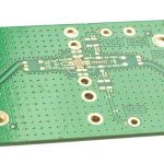
Thick Copper PCB Manufacturing Guide: 4oz Power PCB Boards Explained
A power supply is the core energy source of electronic equipment, so its stability and efficiency directly affect overall system performance. A thick copper PCB with 4oz copper is designed to carry higher current with lower resistance, making it one of the most reliable choices for industrial drives, EV charging systems, telecom base stations, and renewable energy equipment. When high current flows through a board, standard copper thickness may create excessive heat and voltage drop; thicker copper solves both problems.
Where 4oz Thick Copper PCBs Are Used
Heavy copper boards appear wherever a circuit must handle strong current or repeated thermal stress. In industrial control, motor drives and automated production lines use thick copper traces to maintain stable power during long, high-load operation. In automotive electronics, battery management systems and onboard chargers rely on low-resistance paths to reduce energy loss and improve range. Communication base stations operate around the clock and need boards that withstand high-frequency, high-current conditions. Solar inverters and wind power controllers also use PCB manufacturing processes that support heavier copper for more predictable power output.
Materials and Lamination for Heavy Copper Layers
Material selection is the first step in manufacturing a reliable thick copper PCB. FR4 is commonly used as the insulating base because it offers good mechanical strength and electrical insulation. A 4oz copper foil is thicker and stiffer than standard copper foil, so the lamination process must control temperature, pressure, and time precisely. If the copper and substrate do not bond evenly, bubbles or delamination can form and eventually damage the board’s electrical performance and service life. A PCB design and layout review before production helps engineers define balanced copper distribution, thermal reliefs, and panel-friendly trace widths.<

/p>
Etching High-Current Copper Traces
Etching is one of the most demanding stages for heavy copper. Because the copper layer is much thicker, etchant takes longer to penetrate, which increases the risk of undercut and uneven line edges. Manufacturers typically use multiple etching steps to remove copper gradually and form accurate traces. Side etch must be controlled carefully so fine features do not become narrower than the design requires. With strict process parameters, the board keeps clean edges, precise trace widths, and stable current-carrying capability.
Drilling and Plating Reliable Current Paths
Drilled vias connect different copper layers and allow current to flow through the complete circuit network. Heavy copper boards require precise holes and controlled plating thickness so the barrel can handle the intended current. Plating quality is especially important for power boards because thin or uneven plating becomes a weak point under load. Good hole wall quality also supports soldering and long-term reliability.
Surface Finish and Solderability
The final protective stage is surface finish. Common finishes such as ENIG and HASL improve solderability and oxidation resistance. For a thick copper board used in humid or high-temperature environments, the finish must remain consistent across the board so components can be soldered reliably and the copper surface stays protected during storage and operation.
Key Advantages of Thick Copper PCB Boards
The main advantages of a 4oz copper PCB are high current-carrying capacity, excellent heat spreading, and lower electrical loss. A thick copper layer works like an integrated heatsink, pulling heat away from components and helping equipment run cooler. Lower resistance and inductance also reduce signal loss and noise, which is valuable for clean, stable power delivery in sensitive systems.<

/p>
Manufacturing Challenges and Future Improvements
Despite these benefits, heavy copper boards are more difficult to process and usually cost more than standard PCBs. Manufacturers must balance yield, cycle time, and material cost, especially for projects with tight budgets. As electronic products become smaller and lighter, engineers also need thinner constructions that still preserve the thermal and electrical advantages of thick copper. New materials, smarter process control, and automated production are helping manufacturers reduce cost while maintaining quality.
For a high-current or power-related board, working with a manufacturer that understands heavy copper is important. At gopcb, we support projects from early DFM review to prototype PCB assembly and later high-volume PCB assembly, so you can validate performance first and scale production with the same engineering standards.