How to Prevent PCB Short Circuits During the Design Stage
In PCB design and manufacturing, short circuits are among the most common and costly failure modes. A single design mistake can lead to product malfunction, manufacturing scrap, assembly issues, or field failures. The key question is: can short circuits be detected and prevented before fabrication?
The answer is yes. By combining proper PCB Design Rules, systematic verification, and manufacturability analysis, most short-circuit risks can be eliminated during the design stage. This article explains the common causes of PCB short circuits and how engineers can prevent them through good design practices.
One common issue occurs when copper areas belonging to different networks unintentionally overlap.
For example, a via connected to the power negative (V-) net may be placed near manually created copper connected to the power positive (V+) net. If manual copper filling extends into the wrong area, the V+ and V- networks can become electrically connected, resulting in a short circuit.
Modern EDA software such as Altium Designer, Cadence, PADS, and other PCB design tools can normally identify these errors when proper DRC rules are enabled.
For manufacturable designs, engineers should establish appropriate design constraints before routing. GOPCBA also provides professional PCB Layout Design services to help optimize manufacturability and reduce design risks.
A short circuit may occur when vias from different nets overlap physically.
For example:

This creates a direct electrical short between power and ground.
Proper via-to-via spacing rules should always be defined in the PCB design software.
A via connecting Layer 1 and Layer 4 may pass through Layer 2 and Layer 3 without proper clearance.
If anti-pads or isolation areas are not defined, the via barrel may unintentionally contact copper on intermediate layers, causing shorts between unrelated nets.
This problem is especially common in multilayer boards with complex stack-ups. During PCB Manufacturing, these hidden defects can become permanent electrical failures.
Short circuits may also occur when traces, pads, vias, and copper pours do not maintain sufficient spacing.
Typical risk areas include:
These issues can generally be avoided by enabling a properly configured DRC Check system.
Before starting layout, designers should understand the PCB manufacturer’s process capabilities, including:
Design rules should always meet or exceed the manufacturer’s capability limits.
For prototype projects, early collaboration between designers and manufacturers can significantly reduce risks. GOPCBA offers Prototype PCB Assembly services that include DFM review and engineering support.
Good layout habits are essential for preventing shorts.
Visual inspection remains an effective supplementary method, especially for critical nets such as:
A comprehensive PCB Design Rules system should include:
Different net classes should have different clearance values according to voltage, current, and reliability requirements.
In addition to DRC, engineers should perform DFM Analysis (Design for Manufacturability).
DFM tools can analyze source design files or Gerber data from a manufacturing perspective and may identify issues that traditional DRC checks miss.
Typical DFM checks include:
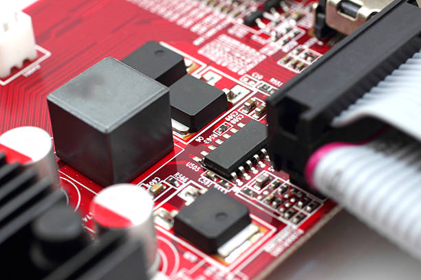
GOPCBA integrates DFM review, engineering analysis, and PCBA Testing to improve manufacturing yield and product reliability.
Preventing PCB short circuits should not rely solely on a final DRC scan.
A reliable process combines:
The most effective strategy is:
Rule-Driven Design + Visual Verification + DRC + DFM + Engineering Review
By implementing this approach, designers can identify potential problems before fabrication, reduce rework, improve manufacturing yield, and increase long-term product reliability.
For complete PCB and PCBA projects, GOPCBA provides one-stop services including PCB Layout Design, PCB Manufacturing, component sourcing, assembly, testing, and quality control.