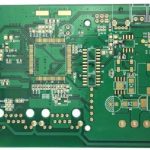
Small SMD Components in PCBA: Why Smaller Costs More
Why do small SMD components in PCBA cost more than larger parts with the same electrical function? The answer is not the material inside the component but the precision required to handle, place, solder, inspect, and test it. Components such as 0201 and 01005 packages can be difficult for older equipment and processes to handle consistently. Higher equipment investment, lower manufacturing margins, stricter supply chain control, and additional inspection all add cost that eventually appears in the PCBA quotation.
This guide explains why miniaturization raises assembly cost, how manufacturers reduce the risk, and what buyers can do to keep high-density PCBA projects within budget.
What Makes Small Components Hard to Assemble
Small SMD components are not simply scaled-down versions of larger parts. Their pads are tiny, their weight is very low, and their tolerance for placement error is extremely small. A 0201 component can be displaced by a tiny movement of the nozzle, a slight vibration, or a difference in solder paste volume.
The machine must accurately recognize each component, pick it from the feeder, position it over the pad, and place it without dragging solder paste. This requires high-resolution cameras, precise motion control, and stable environmental conditions.
As components move from 0402 to 0201 and 01005, the acceptable placement error becomes so small that a machine designed for consumer electronics may not be capable enough. Specialized high-precision placement equipment is needed for reliable results.
Equipment Cost and Cleanroom Environment
High-precision SMT placement machines are more expensive than standard machines because they need better optics, motion systems, feeders, and software. The additional capital cost must be recovered through the assembly price, especially when small components are a small portion of the total board.
Contamination is another issue. Dust or lint under a tiny component can prevent proper contact with the pad. High-end assembly facilities may use controlled or cleanroom areas when building very small packages.
Stencil design also becomes more important. The aperture must deliver the correct amount of paste without creating bridges or voids. Laser-cut stencils and precise stencil printing are common for fine-pitch, small-component boards.
Feeder and tape quality is also part of the hidden cost. A damaged reel, weak pocket, or worn feeder can cause the machine to pick two components, pick one at an angle, or miss one completely. Because 0201 and 01005 parts are so light, static charge can also make them stick to the tape or the nozzle in unexpected ways.
Why Yield Is Lower for Small Parts
A smaller component has less room for soldering error. If the part shifts slightly, one end may not wet correctly, causing a tombstone or open joint. Excess paste can bridge between close pads, while too little paste can leave an insufficient joint.
Even with careful setup, small components can be lost or damaged when a feeder is misaligned or the nozzle creates too much force. Reworking a missing 01005 component is difficult because the part is almost invisible to the human eye.
Because the first-pass yield is lower than for standard components, the assembly process requires more inspection, more rework, and more scrap allowance. These costs must be reflected in the final quote.
The cost difference becomes visible when comparing a board that uses mostly 0603 components with one that uses 01005 parts throughout. The second board may require a different placement machine, smaller stencil apertures, more inspection locations, and a longer setup time. The component price itself is only a small part of that change.
Inspection Challenges
Visual inspection is not enough for 0201 and 01005 components. The solder joints are too small and too close together for an operator to assess reliably. Automated optical inspection with high magnification is needed after placement and reflow.
Solder paste inspection should be performed before placement to verify that each aperture contains the correct paste volume. X-ray inspection may also be used when components are under shields or when hidden solder joints must be checked.
This extra inspection is part of the reason miniaturized PCBA costs more. The manufacturer cannot reduce quality control without increasing the risk that a defective board will reach the customer.
Component verification is especially important when a design depends on tiny packages. A single wrong reel can cause thousands of assemblies to be built with the wrong part, and the error may not be visible until functional test or field use. Incoming inspection and process traceability protect both the buyer and the manufacturer.
Supply Chain and Material Risk
Tiny components are easier to lose, mix, or contaminate during receiving, storage, and kitting. They often come on narrow paper or embossed tape, and a damaged pocket can make the feeder skip parts without being noticed immediately.
MOQ can also be higher because suppliers may not produce small quantities of specialized packages economically. Buying through reliable authorized distributors is important because counterfeit or recycled tiny components are especially dangerous in high-density designs.
Inventory management must keep different reel lots separate and maintain proper storage conditions. Small parts are sensitive to moisture and can oxidize if exposed to humid air for too long.
A strong component procurement team can help buyers source, verify, and manage these parts more efficiently.
Miniaturization often happens together with other advanced features such as fine-pitch BGAs, microvias, and thinner boards. The assembly process must then manage multiple risk factors at once. This is why a project with small components and high-density HDI structure should be planned as a complete manufacturing challenge instead of treating each feature separately.
PCB Design and DFM Impact
Small components force designers to use tighter pad spacing and finer routing. This can increase PCB layer count, reduce trace width, and create more complex manufacturing requirements. A small component placed between two BGAs may also make rework access almost impossible.
DFM analysis should check whether the pad size, stencil aperture, component spacing, and thermal relief are suitable for the selected package. If the design leaves too little room for solder mask or placement, yield will suffer.
Designers can keep cost under control by using the smallest component only where board space truly requires it. In areas with enough room, a slightly larger package may improve yield, reduce inspection effort, and lower total cost. Early PCB design and layout review helps make that tradeoff clear.
Board thickness and component density also change the amount of heat absorbed by each joint. Small components on a thin board may reflow faster than larger parts on a thick power board. The reflow profile should therefore be developed for the actual product, not copied from another project.
Soldering Process Control
Reflow profiling is critical for small components. The peak temperature, time above liquidus, and cooling rate must match the solder paste and the thermal mass of the board. A profile that works for a large power component may overheat a tiny resistor or cause a solder ball.
Nitrogen reflow can reduce oxidation and improve wetting, but it adds cost. It may be justified for fine-pitch and small-component boards that are difficult to solder reliably in air.
Double-sided assembly introduces another complication. Small parts on the bottom side must remain in place during the second reflow, or the assembly order must be changed to protect them.
Quality and Reliability Expectations
Small components are used because they allow high-density design, not because they improve reliability by themselves. In fact, they may be more sensitive to thermal stress, mechanical flex, and contamination than larger parts with thicker solder fillets.
Quality control should include solder joint inspection, electrical test, and, for high-reliability applications, X-ray sampling or full inspection. Functional test is still needed because a visually perfect board can contain an electrical failure.
A complete SMT PCB assembly flow with PCBA testing is the most effective way to verify that miniaturized boards meet the specification.
How to Reduce Cost in High-Density PCBA
Use small components only where they are necessary. If the board has unused space, a larger package can reduce assembly risk without changing performance. Standardize the component list across similar products to simplify sourcing and process setup.
Work with the assembly partner during design to understand placement, stencil, and inspection capability. This prevents designs that cannot be built reliably at the planned cost.
Plan the test strategy early. Adding small test points, avoiding components under test areas, and keeping programming interfaces accessible can reduce the cost of ICT and FCT.
Before choosing a very small package, compare the total manufacturing cost with a slightly larger alternative. A larger component may require a few extra square millimeters of board area, but it can reduce placement difficulty, inspection requirements, and rework risk enough to lower the final project cost.
Conclusion
Small SMD components in PCBA cost more because they require precision equipment, controlled environments, lower yield tolerance, stronger supply chain control, and more inspection. The real price of miniaturization includes not only the component itself but the entire manufacturing system needed to handle it.
With careful design, realistic component selection, and a manufacturer that has qualified small-package processes, companies can benefit from high-density PCBA without paying more than necessary.