Embedded Passive Components PCB: Design and Benefits Guide
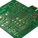
An embedded passive components PCB places resistors, capacitors, inductors, or combinations of these parts inside the board structure instead of mounting them on the surface. This technology helps manufacturers increase circuit density, improve signal performance, and reduce assembly problems. As electronics become thinner, faster, and more integrated, embedding passive components is becoming an important option for high-density and high-frequency designs.
This guide explains the types, applications, benefits, and manufacturing considerations of embedded passive PCBs.
Embedding is most useful when the board contains many repeated resistors, capacitors, or termination components that have stable design values.
Why Embed Passive Components
Modern products place thousands of passive components on the PCB surface. These parts use significant area and add many solder joints that can fail over time.
Embedding passives moves some of those components inside the PCB layers, freeing surface area for active devices and reducing the distance between connections.
The result is a more compact board with shorter signal paths and better electrical performance.
Embedded components are usually formed from special layers that are laminated into the PCB stackup. Their values are controlled by material thickness, pattern geometry, and process parameters.
Types of Embedded Passive PCBs
Embedded resistor PCBs contain resistive elements formed inside the board. Embedded capacitor PCBs include capacitive structures in the internal layers.
Embedded inductor PCBs place inductive elements within the laminate, while a board with several types is called an embedded passive PCB.
Each type requires different materials, imaging methods, and fabrication steps in the PCB stackup.
Embedded passives are also used in automotive radar, medical imaging, and wireless modules where small size and stable high-frequency behavior are important.
Applications
Embedded passive technology is used in high-performance computers, communication systems, portable devices, test instruments, aerospace electronics, and medical equipment.
It is especially useful for RF modules, signal processors, and high-speed boards where parasitic effects can distort signals.
Many boards benefit from reducing the number of discrete passives on the surface.
When a large number of resistors are used for termination, filtering, or pull-up circuits, embedding them can reduce surface congestion and simplify the placement process.
Increasing Board Density
Passive components occupy a large percentage of the PCB surface in dense products. A mobile phone board may contain hundreds of small passives.
Embedding a portion of these components can reduce the required board area and the number of surface connections, sometimes by a significant amount.
Higher density gives designers more room for active chips, connectors, and other functions.
Reducing surface solder joints also reduces the number of locations where opens, bridges, and solder fatigue can occur during service.
Embedding also reduces the number of components that the placement machine must handle, which can shorten cycle time and lower the chance of a missing or misplaced part.
Improving Assembly Reliability
Each surface-mounted passive adds a solder joint that can be damaged by heat, vibration, or mechanical stress. Embedded passives reduce the number of exposed solder joints.
The internal components are protected from moisture, contamination, and handling damage.
This can improve long-term reliability in products used in harsh environments.
Power integrity can also improve because decoupling capacitors can be placed closer to the power and ground planes with lower loop inductance.
Embedded components can also reduce electromagnetic interference by shortening high-frequency current paths and reducing loop area.
Improving Electrical Performance
Discrete passive components have connection pads, wires, and solder joints that introduce parasitic inductance and capacitance. Embedded passives reduce these effects by shortening the electrical path.
Shorter connections improve signal integrity, reduce parasitic inductance, and reduce distortion at high frequency.
Embedded components are also protected from changing environmental conditions, helping their values remain stable.
The cost comparison should include the board, assembly, rework, reliability, and field failure cost over the life of the product.
Material costs may be higher, but fewer discrete parts, less assembly time, and better first-pass yield can create a favorable total cost.
Saving Product Cost
Although embedded passive technology requires special materials and processes, it can lower total product cost in the right application.
Fewer surface components reduce assembly time, solder cost, and rework risk. A smaller PCB also uses less material and can fit in a smaller enclosure.
Studies of RF circuits suggest meaningful savings in component, substrate, and assembly cost when embedding is used effectively.
The embedded layer must survive multiple lamination cycles without changing its electrical properties. Material qualification is therefore a necessary step.
Material and Process Requirements
Embedded resistor materials must provide stable resistance after lamination. Embedded capacitor materials must have controlled dielectric properties.
The board manufacturer needs special laminates, imaging processes, and testing methods to verify embedded component values.
Tolerances, repeatability, and thermal behavior should be validated with test coupons before mass production.
Layout tools and simulation software should be used to predict the effect of embedded passives on signal integrity and impedance before fabrication begins.
The designer should also plan for thermal effects because embedded resistor layers may have a different temperature coefficient from discrete parts.
Design Considerations
The design must account for the value and tolerance of embedded components. Resistance and capacitance may vary through the lamination process.
The board layout should include test access and registration targets for measuring embedded values and layer alignment during production.
Designers should work with the manufacturer early to define material properties and process capability.
At high frequency, even short leads from a discrete passive can create unwanted reactance. Embedded components reduce that reactance by placing the part in the current path.
HDI and High-Frequency Boards
Embedded passives are often used with HDI technology. The combination supports small vias, high density, and short connections.
RF designs can reduce loss and parasitic effects by placing matching components near the active circuit.
High-speed digital boards can benefit from improved power integrity and reduced signal distortion.
Because the passive layers are embedded, they are not exposed to assembly flux or cleaning chemicals in the same way as surface parts.
Reliability and Environmental Protection
Embedded components are located inside the board where they are less exposed to moisture, chemicals, and mechanical damage.
This protection can reduce corrosion and improve stability over the product’s service life.
For medical, aerospace, automotive, and military applications, this protection is an important reliability advantage.
An integrated design and manufacturing review is important, and PCB design and layout engineers should be involved before final stackup release.
The factory should provide a DFM review that identifies process limitations such as minimum embedded resistor size, registration, and thickness variation.
Manufacturing Capability
Embedded passive PCB production requires advanced fabrication equipment and process experience. The factory must control material, lamination, imaging, and electrical test.
First article verification is important because embedded component values cannot be reworked after lamination.
A capable PCB manufacturing partner should provide engineering feedback during design.
Electrical testing should be combined with PCBA testing to confirm that the embedded values support the function of the assembled module.
Test coupons on the production panel should match the embedded layer stackup so they represent the actual component values on the board.
Testing Embedded Components
Embedded resistors, capacitors, and inductors must be measured during production. Test coupons can verify material behavior before the final board is built.
The final board should be electrically tested to confirm that all embedded values are within tolerance and that layer-to-layer connections are reliable.
Functional test after assembly provides an additional quality check.
Prototype validation is strongly recommended before a high-volume order because embedded layers cannot be changed easily after lamination.
Comparing embedded technology with a conventional multilayer or HDI solution requires data from both board cost and assembly yield studies.
The final decision should be based on board size targets, expected signal frequencies, reliability goals, production volume, and the manufacturer process capability.
Choosing the Right Technology
Embedding passive components is not suitable for every product. The decision should compare density, reliability, electrical benefit, cost, and manufacturing risk.
For high-volume consumer boards, the cost may not justify the extra process. For advanced RF and high-reliability products, the benefits are greater.
A controlled SMT PCB assembly process should be used for the remaining surface components.
Working with an experienced partner that can simulate, fabricate, test, and assemble embedded passive PCBs reduces the risk of the technology.
Embedded passive technology should be considered when surface density, signal performance, or reliability creates a clear requirement that conventional assembly cannot meet.
Embedded passive PCBs are becoming more practical as materials and design tools improve, but they are not yet the standard choice for every board.
Suppliers should provide clear data about yield, tolerance, and reliability so the customer can make an informed decision between embedded and conventional assembly.
As fabrication technology matures, embedded passive PCBs will become more accessible for a wider range of electronic products.
Engineers who understand embedded passive technology can use it to create smaller, faster, and more reliable products when the application justifies the process.
Conclusion
An embedded passive components PCB improves density, reliability, electrical performance, and potentially cost when the design is suitable.
Manufacturers should evaluate material stability, process control, testing, and assembly integration before selecting this advanced technology.