PCB Tooling Holes and Panel Design
What Tooling Holes Are For
A tooling hole is a non plated hole that a machine or a fixture uses to locate a board or a panel mechanically. Fiducials tell a vision system where the board is; tooling holes physically hold it there, and the two work together. They are used on the panel so that every process step from inner layer imaging onward can register to the same datum, and they are used on the finished board so that test fixtures, assembly fixtures, machining operations and enclosures can locate it in the same place every time. A board with no tooling holes is located by its outline, which varies with the routing tolerance, so a fixture that clamps on the edge can shift by a few tenths of a millimetre between units, which is enough to ruin a placement or a test.
Panel Tooling Holes
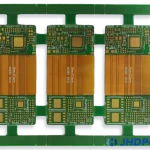
Panels carry tooling holes in the border, and they are the datum for the whole manufacturing sequence. Their diameter is normally between three and four millimetres, and the position tolerance is tight, because every subsequent layer is registered to them: a small error in the tooling hole position translates into a registration error at every layer. They are usually arranged asymmetrically so that a panel cannot be loaded the wrong way round, and they are placed outside the board area so the finished product does not inherit them. The number and position are normally proposed by the fabricator, and the designer’s only responsibility is to leave enough border to accommodate them and the fiducials.
Board Level Tooling Holes
When the assembly, test or enclosure needs to locate the finished board, the holes must be designed into the board itself. A common arrangement is two holes on one long edge and one on the opposite edge, or two on the diagonal, so that the board is constrained in translation and rotation while still being easy to load. The diameter is chosen to suit the fixture pin, usually with a small clearance so the board drops on rather than being forced, and the position tolerance should be stated, typically plus or minus 0.05 to 0.1 mm relative to the board datum. Non plated holes are the norm, because plating adds a thickness variation and a burr; where a plated hole must be used, the finished diameter after plating is what matters.
Interaction With Components and Copper
A tooling hole is a hole, so it needs a keepout: copper and solder mask should be kept clear of the hole by at least the process allowance, and no component or trace should sit within the area that the fixture pin or the clamp will occupy. That area is often larger than the hole itself, because the fixture may have a boss around the pin. Care is needed where the tooling hole is close to a component that will be placed before the fixture is used, because the fixture landing on a component is a defect that appears intermittently and is difficult to trace. Where the board will be machined or milled after assembly, the tooling holes are the datum for that operation as well, which usually means they should be present before assembly rather than added afterwards.
Tolerances and Datum Practice
The productive way to think about tooling holes is as a datum definition. Choose the datum first, then dimension everything that matters from it: the outline, the fiducials, the connector positions and the tooling holes themselves. If the drawing dimensions the outline from one edge and the holes from another, the fabricator has to infer the relationship, and the resulting stack of tolerances can exceed the requirement. In practice this means the drawing should define a primary datum from the tooling holes, and the outline tolerance should be a consequence of the routing process rather than the reference for everything else. Where a mechanical interface is critical, such as a press fit connector or a board that mates with a housing, that interface should be dimensioned from the tooling holes rather than from the outline.
Cost and Design Errors
Tooling holes cost almost nothing to add when the panel is designed and can cost a great deal to add later, because the finished board cannot easily be drilled without risking the copper and the components. The common mistakes are placing a hole where a component or a fixture boss will need space, using a plated hole where a non plated one is required, giving no position tolerance so the fabricator works to its default, and assuming that the outline is a precise datum when it is the least precise feature on the board. Each of these is visible in a design review with the fixture drawing on the table, and invisible if the review only looks at the circuit.
FAQ
How many tooling holes does a board need? Enough to constrain translation and rotation, usually three arranged asymmetrically so that the board can only be loaded one way.
Should tooling holes be plated? Normally not. Non plated holes avoid the plating thickness variation and the burr, and they are easier to hold to a diameter tolerance.
What tolerance should be specified? Around plus or minus 0.05 to 0.1 mm relative to the datum, tighter where the fixture, a connector or a machining operation depends on the position.
How big should the keepout around a tooling hole be? Larger than the hole, because the fixture pin usually sits in a boss or a bushing. Allow for the fixture hardware, not just the pin.
Are tooling holes the same as fiducials? No. Fiducials are optical marks for vision alignment; tooling holes are mechanical features that hold the board in position.
Conclusion
Tooling holes define the datum that the rest of the mechanical design hangs from, so they should be chosen deliberately rather than inherited from a template. Keep them non plated, give them a realistic diameter and a stated position tolerance, allow for the fixture hardware rather than only the pin, and dimension every critical interface from them rather than from the outline. The panel and drilling capabilities available are part of PCB capabilities, the mechanical conventions belong in PCB design and layout, and the assembly and test stages that use the holes are covered by PCBA testing. A prototype PCB assembly run with the real fixture confirms the location before volume in 2026.