Impedance Coupon Design and Placement
Why a Coupon Exists
Controlled impedance cannot be measured on a finished product board in any practical way: the traces are under components, the reference planes are buried, and the geometry that must be verified is inside the laminate. The industry solution is to build a coupon alongside the boards on the same panel, using the same stackup, the same imaging, the same etching, the same lamination and the same plating, and to measure that instead. The coupon is therefore not a sample of the product; it is a witness that the process that produced the product was behaving correctly. When the coupon data is supplied with the panel, it is the evidence behind an impedance claim.
What Belongs on the Coupon
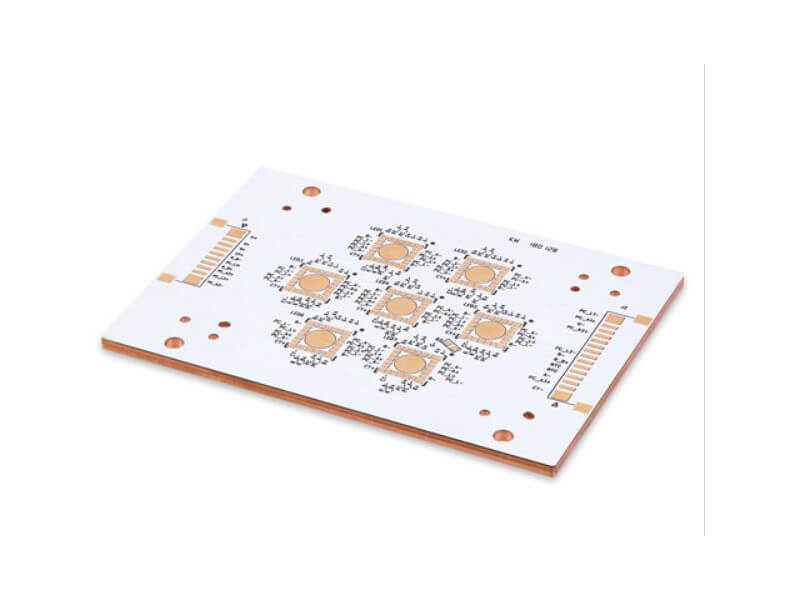
A useful coupon carries a test structure for every impedance requirement in the design, each one built at the same nominal geometry as the corresponding trace on the product. A single ended structure for each target impedance, usually fifty ohms, a differential structure for each differential target, commonly ninety or one hundred ohms, and any other controlled geometry such as coplanar or edge coupled lines. Each structure should include the same stackup, the same copper weight and, importantly, the same reference planes as the product traces it represents, because the reference is half of the transmission line. The coupon also normally carries test points at both ends sized for the measurement probe or for the connector, a ground reference adjacent to each signal, and identification marking so that a measurement can be traced back to the structure it came from.
Length, Launch and Measurement
The measurement is made with a time domain reflectometer or a vector network analyser, and both are sensitive to the quality of the launch. The structure should be long enough that the travel time is clearly separated from the launch discontinuity and the end reflection, typically a few centimetres, and the launch should be a defined geometry rather than an arbitrary pad. Where a high frequency measurement is needed, the coupon is often fitted with a coaxial connector footprint so the probe or cable can be attached with a defined reference plane. Ground pads must be close to the signal pad for a good launch; a signal pad with a distant ground forces the probe to form a long loop and the measurement degrades. The coupon should also avoid structures that are coupled to each other, since neighbouring traces change the measured impedance.
Placement in the Panel
The coupon has to be placed where it experiences the same process as the boards, and that is not necessarily the same place in every panel. Etching is not perfectly uniform across a panel, and plating current density varies with position, so a coupon in the corner may read differently from a trace in the middle. The common practice is to place the coupon on the panel border, oriented the same way as the boards so that the traces run in the same direction relative to the laminate weave, which affects the dielectric constant. Where the design is critical, more than one coupon can be placed at different positions to show the spread across the panel, which is more informative than a single measurement.
Reading the Data
The measurement reports an impedance with a tolerance, and the qualification question is whether the process is centred on the target and whether the spread is inside the specification. A coupon that reads two percent high on every panel suggests the model or the artwork compensation is slightly off and should be corrected rather than accepted. A coupon that varies between panels suggests a process drift, which is a different problem and is addressed differently. Because the coupon is built on the panel, the same measurement also confirms the dielectric thickness and the copper thickness indirectly, and a cross section of the coupon area is a useful complement: it shows the actual dimensions behind the electrical result.
How to Specify It
The fabrication drawing should state the impedance targets with tolerances, the coupon location and size, the structures required, the measurement method and the reference plane for each structure. It should also state what is to be reported and with what, since a number without a method is not evidence. Where the design is high volume, the sampling should be defined: every panel, every lot or a defined frequency. And where the requirement is tight, the drawing should say what happens when a panel is outside the tolerance, because a supplier that has no defined action will ship the panel and mention it afterwards.
FAQ
Why can impedance not be measured on the product board? Because the traces are buried under components and reference planes, and the geometry that determines the impedance is inside the laminate. The coupon is built with the same process and measured instead.
How long should a coupon trace be? Long enough to separate the launch and end reflections from the measurement, typically a few centimetres, with a defined launch geometry at each end.
Where should the coupon be placed? On the panel border, in the same orientation as the boards, and where the design is critical at more than one position so that the spread across the panel is visible.
Does coupon data prove every board is compliant? It proves that the process was behaving to specification for that panel. It is process evidence rather than a measurement of each trace.
What happens if a coupon is out of tolerance? That should be defined in the drawing, because without a stated action the panel may be shipped with a note rather than rejected.
Conclusion
The impedance coupon is the only practical way to prove that a controlled impedance design was built as specified, so it should be designed as carefully as the product: the right structures, the right reference planes, a good launch, a sensible length and a placement that experiences the real process. State the targets, the tolerances, the measurement method and the disposition rule in the drawing, and read the data for trends as well as for pass or fail. The stackup and process limits behind the coupon are part of PCB capabilities, the trace geometry that the coupon reproduces belongs in PCB design and layout, and the etching and lamination steps that the coupon witnesses are described in PCB manufacturing. A prototype PCB assembly build with coupon data is the cheapest way to confirm a high speed stackup before volume in 2026.