Open Drain Signalling: How I2C Returns to High Without a Driver
A logic bus where no device ever drives a high level sounds like a design error. Every participant can only pull the line low, and yet the line reliably returns to a valid high level, which is the basis of I2C and of many other shared control buses. The mechanism is the pull-up resistor, and understanding it explains most of the practical limits of the bus.
Open drain signalling is not a curiosity. It is the reason multiple devices can share a bus without destroying each other, and the reason that bus speed depends on layout capacitance.
How an Open Drain Output Works
An open drain output contains a transistor that can connect the line to ground and nothing that can connect it to the positive supply. When the transistor is off, the output is effectively an open circuit. When it is on, the output pulls the line down.
The high level is provided externally by a resistor connected to the supply rail. With no device pulling down, the resistor charges the line to the supply voltage, and the bus reads as a logic one.
Two consequences follow immediately. First, the rise of the signal is an RC charging curve given by the resistor and the total capacitance of the line, so the rise time is set by the designer rather than by a driver. Second, the fall is driven by the transistor and is usually much faster than the rise.
That asymmetry is visible on any scope trace of an I2C bus and is the first thing to check when the bus behaves intermittently.
Why a Shared Bus Is Wired This Way
The architecture solves a problem that would otherwise require arbitration in hardware: two devices driving the same line in opposite directions would create a short circuit and potentially damage both.
With open drain outputs, the worst case is that both devices pull low, which is harmless. The bus behaves as a wired-AND function, and that property is what allows a multi device bus to work at all, including the clock stretching that a slow device can use to delay a transaction.
It also makes level translation simple. Devices supplied from different rails can share the bus if the pull-up is connected to the lowest of the relevant supplies, or if a dedicated translator is used, because no device is ever required to source current into the line.
A multi device bus therefore has one resistor, or one pair of resistors, and any number of participants, with the constraint that the total capacitance and the equivalent resistance have to remain within the limits the protocol specifies.
Choosing the Pull-Up Resistor
The I2C pull up resistor is chosen by two competing limits: it must be small enough to charge the bus within the rise time the protocol allows, and large enough not to exceed the current that a device can sink when it pulls the line low.
The rise time calculation is an RC problem. For a bus with total capacitance Cb and pull-up resistance Rp, the rise time is approximately 0.8473 times the product of the two, and the standard places an upper limit on that value depending on the bus speed.
Bus capacitance comes from several places: the pin capacitance of every device, the capacitance of the traces, the connector if the bus leaves the board, and any cable. A bus with ten devices and a cable to a remote board can accumulate a capacitance that forces a much smaller resistor than a two device bus on the same board.
The lower limit is set by current. A device pulling the line low must sink the current flowing through the resistor while keeping the voltage below the specified low level, and that current is simply the supply voltage divided by the resistance. Too small a resistor increases power consumption and may exceed the sink capability of the weakest device on the bus.
Layout Consequences That Are Frequently Underestimated
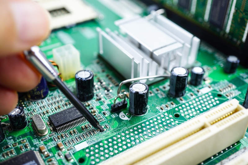
Because the bus is capacitive and the rise is resistive, the layout directly determines whether the bus will meet its timing.
Long traces add capacitance, which slows the rise. Stubs add capacitance without carrying the bus anywhere useful, so the recommended practice is to route the bus as a daisy chain through the devices rather than with branches. A connector adds capacitance and often a cable, which is why buses that leave the board need a smaller resistor or a bus buffer.
The ground return matters for the same reason as in any signal integrity discussion. A bus that is routed without a nearby return has a higher inductance and a larger loop area, which degrades the edges and increases emissions.
Protection is part of the same decision. A bus that leaves the enclosure is exposed to electrostatic discharge and to accidental shorts, and series resistors or dedicated protection devices should be placed so that the disturbance is handled before it reaches the devices. Where components are selected for that role, the bus capacitance of the chosen protection matters as much as its clamping voltage.
Practical Checklist
- Count the total bus capacitance: device pins, traces, connector and cable.
- Compute the rise time from the resistance and capacitance, and compare it with the protocol limit.
- Check that the smallest device can sink the current the resistor allows at the specified low level.
- Route as a chain rather than a star, and keep stubs as short as possible.
- Provide a return path alongside the bus on the same layer stack.
- Protect any segment that leaves the board, and account for its capacitance.
- Measure the actual rise and fall times on the prototype rather than relying on the calculation.
Verifying the bus on a real prototype is inexpensive and conclusive. A scope trace of the clock and data lines will show the rise time, any rounding caused by excessive capacitance, and any asymmetry that suggests the resistor has been chosen for the wrong bus load. Where the board is built and tested by a partner that also performs PCBA testing, that measurement can be part of the first article rather than a separate investigation.
FAQ
Why not use a push-pull driver instead? Because two devices could then drive the line in opposite directions and create a short circuit. Open drain avoids that by construction.
Can the pull-up be placed anywhere? Electrically it can be placed at one point on the bus, and physically it should be placed where it best serves the load, typically near the middle or at the master for a simple two device bus.
What happens if the resistor is too large? The rise becomes too slow and the bus fails timing, particularly with a long trace or a cable.
What happens if it is too small? Current increases, power rises, and a device may not be able to hold the low level within specification.
Summary
Open drain signalling explains both the robustness and the limits of I2C: the line returns high through a resistor, so the rise time calculation is a function of the I2C pull up resistor and the bus capacitance. Choose the resistor from both ends of the constraint, route the multi device bus without stubs, and confirm the result on a measurement rather than on the schematic.