




Multilayer PCB Manufacturing: Registration, Lamination and Drilling
Multilayer boards are not simply conventional boards stacked up. The number of layers, the thinness of the dielectric between them, the density of the routing, the number of holes and the size of the panel all combine to make a different set of processes critical. Four of them decide whether a design can be built to the tolerance it was drawn to.
A designer does not need to run a plating line to work with them, but understanding where the difficulty sits is what makes a design manufacturable rather than merely legal. Most of the constraints that matter can be respected while the layout is still a file.
Layer to Layer Registration
Each layer is imaged on its own core, and the layers are aligned to each other when the stack is laminated. The tolerance of that alignment is measured in tens of microns, and it has to accommodate several contributions: the dimensional behaviour of the cores themselves, the difference between cores from different batches, the humidity and temperature of the imaging area, and the method the shop uses to locate each layer.
Large panels make this harder, because a small dimensional error in one direction accumulates across the panel. So does a design with tight annular rings and small holes, where the remaining copper between the hole wall and the pad edge is the quantity that absorbs the misregistration. When the alignment budget is consumed, the failure is not graceful: pads break out of their annular rings, and vias that were electrically connected become marginal.
The design side of this constraint is straightforward. Specify the standard tolerance recorded in the fabrication capability and choose annular ring dimensions that survive it, rather than assuming the nominal case. Where a stack uses several different core thicknesses, expect the stack to move more than a uniform one.
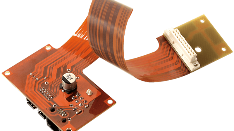
Inner Layer Imaging and Etching
Inner layers are imaged and etched before lamination, and the materials used in high performance boards make that step harder. High glass transition temperature laminates, high frequency materials, thick copper and thin dielectric substrates each behave differently under exposure and etch, and the combination of them is what most modern designs contain.
Thin cores are the most awkward. A very thin inner layer is mechanically flexible and wrinkles easily, which produces exposure defects, and it can curl as it passes through the etching equipment. Thinner traces and narrower gaps raise the probability of opens and shorts, and a layer carrying dense fine geometry has more opportunities for a defect that the automated optical inspection might miss only rarely, which is why the inspection thresholds matter.
Large panels carrying expensive, long fabrication cycles make scrap at this stage costly. A defect discovered after lamination has consumed the material and the process time of every layer beneath it, so the value of catching a defect early is higher than the arithmetic suggests.
Lamination
Lamination is where the inner cores and the prepreg sheets are combined under heat and pressure. The defects that appear here are characteristic: layer slip, delamination, resin starvation in areas with little copper, and voids or bubbles trapped in the stack. Each of them relates to the balance of the design and to the schedule used to press it.
The material specification matters. The heat resistance, the resin content, the flow behaviour and the dielectric thickness of each prepreg sheet all influence how the stack consolidates, and a pressing schedule developed for one construction does not transfer to another. Where a layer has very little copper, the resin has more volume to fill, and a stack that was acceptable with a more uniform copper distribution can starve.
Consistent expansion and contraction is the second problem. With many layers, the compensation applied to the artwork for dimensional change cannot be uniform across the panel, and thin insulating layers between the copper planes reduce the mechanical margin. The result is a stack whose inter layer reliability is more sensitive to the process than a two or four layer board would be.

Drilling
Drilling a multilayer board is harder than drilling a thin one for reasons that compound. The total copper thickness and the total thickness of the board both increase, so the drill has more material to pass through and more opportunity to break. Dense BGA areas produce closely spaced holes whose walls are separated by a small amount of material, which is the condition under which conductive anodic filament growth becomes a reliability risk rather than a theoretical one.
Special laminates raise the difficulty further. High glass transition materials, high frequency materials and thick copper all affect the roughness of the drilled wall, the amount of burr produced, and the difficulty of removing the smear left by the drilling operation. A wall that is not clean and desmeared properly will not plate reliably, and the fault may not be visible until the board is in a thermal cycling test.
Board thickness also interacts with hole position. A deep hole drilled at an angle to the surface plane will not land where the design intended, and the error grows with the aspect ratio. The usual design response belongs in the design rules: keep the aspect ratio inside the shop capability, and to specify the tolerance explicitly when the design approaches the limit.
Working With the Constraints
None of this requires the designer to model the process, but it does require the design to be checked against it. Confirm the registration tolerance and design the annular rings for it. Confirm the minimum line width and spacing for the copper weight being used rather than for a nominal figure. Keep the copper distribution reasonably even so that the stack consolidates predictably. Keep the drill aspect ratio, the hole to hole spacing in BGA areas and the smallest hole inside the capability of the shop that will build the board.
Speaking to the fabricator before the stack-up is frozen is the cheapest step in the whole process. A stack-up that assumes a capability the shop does not have will be adjusted during production, and the performance the design was verified against will not be the performance delivered. Where the design is also assembled elsewhere, the same numbers have to be communicated to the assembly partner, since the finished thickness, the flatness and the hole finishes all affect the assembly process.
FAQ
What is a typical layer to layer registration tolerance? It is commonly specified in the tens of microns and depends on the shop, the panel size and the number of layers, so it should be confirmed rather than assumed.
Why is resin starvation a design issue? Because it depends on how much copper is present on each layer. A layer with very little copper leaves more volume for the resin to fill.
What is CAF and why does hole spacing matter? Conductive anodic filament growth is a failure mechanism along the material between two holes, which is why the wall to wall spacing is a reliability parameter rather than only a routing constraint.
Can a thin dielectric layer be used anywhere? It can, but it reduces the mechanical margin of the stack and demands tighter control of the lamination process.
Summary
Multilayer PCB manufacturing is difficult in four specific places: aligning many layers to each other, imaging and etching thin cores with fine geometry, consolidating a stack without voids or starvation, and drilling through more material with closer holes. Each has a design counterpart, and each is best addressed by confirming the fabrication capability before the design is released.