Panelization for Assembly: V-Cut, Tabs and Tooling Strips
Surface mount lines handle panels, not single boards. A bare board that is 60 mm by 40 mm cannot be fed through a printer, a placer and a reflow oven on its own, so it is built as part of an array that carries the same board several times, surrounded by the features the machines need. Designing that array is what panelization means, and the decisions in it affect yield, cost and how cleanly the boards separate at the end.
Two Panels, Two Purposes
The word covers two different things, and confusing them causes most of the arguments about who should do the work.
The fabrication panel is the array the board shop builds from the single board image. The customer supplies one board and the shop repeats it to fill a standard working panel. Nothing on the customer’s side changes, and the cost is driven by the panel utilisation.
The assembly panel is the array that goes through the SMT line. It has to match the conveyor width, carry the fiducials the placement machines use, and hold the boards in a way that survives the reflow profile. This is the panel that has to be designed, and it is the one this article is about.
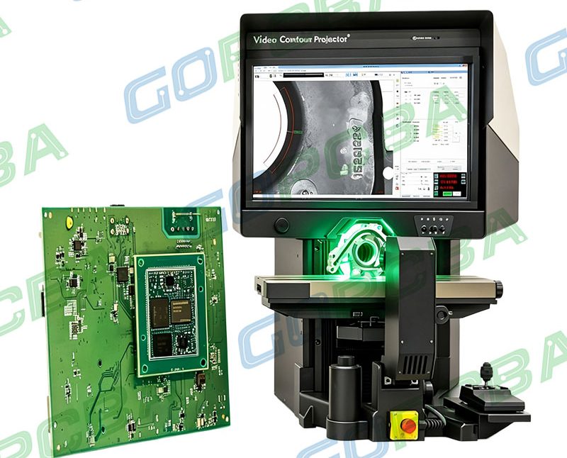
<img src="https://www.gopcba.com/wp-content/uploads/2026/08/Quick-Turn-Printed-Circuit-Boards.png" alt="PCB array with tooling strips and fiducial marks” />
What an Assembly Panel Contains
Four groups of features are needed, and each has a reason.
The array is the repeated board image. The number of boards and their arrangement is set by the panel size the line can handle and by the board outline, and a rectangular arrangement with a common orientation is easier to program and to inspect than a mixed one.
The tooling strip is the border of material around the array that the machines hold. A strip of about 5 mm on the long edges is the usual starting point, and it has to be wide enough for the conveyor rails to support the panel without touching the components. The strip also carries the fiducial marks: three small copper features with the mask cleared around them, placed asymmetrically so that a machine can determine orientation as well as position. One millimetre of copper dot is a common size, and finer pitch work usually adds local fiducials beside the fine pitch devices.
The separation features are what allow the boards to be snapped out. A V-cut is a scored line on both faces of the panel that leaves a thin web of material, and the boards separate when the panel is flexed. A breakaway tab is a small bridge of material between the board and the frame, usually with a row of closely spaced perforations that define the break line. V-cut is fast and cheap and leaves a clean edge on straight sides; tabs are needed where the board edge is not straight, where components sit close to the edge, or where the panel is thin.
The strip also carries the mechanical reference features: mounting holes for the tooling, typically a 3 mm non-plated hole in a defined position, and often an identification mark or a barcode for traceability.
Design Rules That Prevent Problems
The rules that matter are mostly about clearance and rigidity.
Keep components away from the separation line. A part placed within a few millimetres of a V-cut can be damaged by the cutting wheel, and a part beside a tab can be cracked when the tab is broken. The clearance applies to tall parts as well, because the depanelising tool has to reach the line.
Keep the array stiff enough to hold its shape. A thin board in a large array sags in the reflow oven, and a sagging panel has different thermal contact on different boards. Adding rails, keeping the array square rather than long and narrow, and using a sensible rail width all help. The panel drawing is reviewed together with the fabrication data so that the array and the rail width match the working panel the shop actually uses, which the PCB manufacturing review covers. Where the board is flexible, the panel becomes a mechanical design problem rather than a layout convenience.
Keep the thermal mass even. If one position in the array carries the large processors and another carries only small parts, the two boards heat at different rates. The usual fix is to distribute the heavy components consistently so that every board in the array has the same thermal profile, which may mean choosing an arrangement that is not the one that fits most boards per panel.
Check the direction of the connectors and the orientation of the parts. A connector that overhangs the board edge can collide with the neighbouring board in the array, and a connector that faces outward at the panel edge can interfere with the conveyor. The common convention is to orient every board the same way, which also makes the placement programme simpler.
<img src="https://www.gopcba.com/wp-content/uploads/2026/09/78.jpg" alt="V-cut score line and breakaway tab on a panel” />
V-Cut Against Tabs
The choice between the two separation methods is usually made by the board outline.
A rectangular board with straight sides, no components near the edge and a thickness above about 0.8 mm is a natural candidate for V-cut. The scoring depth is commonly a third of the board thickness on each face, leaving a web that breaks cleanly. The constraints are the straight edge and the fact that the cut removes material, so an edge that must be continuous or that carries a plane to the very edge cannot be scored.
A board with a curved outline, a connector at the edge, or a very thin profile needs tabs. The tabs are routed rather than scored, so the edge is cut cleanly, and the perforation pattern sets how the tab breaks. The trade-off is that the separated board carries small burrs where the tab broke, which has to be acceptable for the product or removed by a finishing operation. Tab width and perforation size are process parameters that the assembly partner chooses, because they depend on the router bit and on the depanelising method.
Practical Working Method
There is a shortcut worth knowing when a panel has to be created quickly from an existing single-board design. The array does not need a full copy of the board nine times over, because the fabrication data is generated per board rather than per panel. What the panel needs is the board outline repeated in the correct positions, together with the tooling strip, the fiducials, the separation features and the mechanical holes. Creating a copy of the outline, placing it, and using the original for the electrical data keeps the file small and makes the intent obvious.
Where the panel is produced by hand in a layout tool, the arrangement is therefore a set of outlines and mechanical features rather than a set of repeated circuits. Where the panel is produced by the fabricator, the instruction is a drawing with the array dimensions, the separation method, the fiducial positions and the rail width, and the shop builds the array from the single board data.
The panel is also where the assembly programme is set up, so the panel data has to reach the assembly partner in a usable form together with the placement file. Our SMT assembly team works from the panel definition and the array drawing, and the marking of individual boards for traceability is decided at the same time. Where a board is intended for a small pilot run, the same panel design is used in our rapid prototyping builds so that a later volume run does not need a different panel.
FAQ
Who designs the panel, the designer or the manufacturer? The assembly panel is normally agreed with the assembly partner, because it has to match the line. The fabrication panel is the board shop’s responsibility.
How wide should the tooling strip be? Around 5 mm on the conveyor edges is a common starting point, with the final value set by the line and by the height of the parts near the edge.
Can V-cut be used on a board with a curved outline? No. V-cut requires a straight edge, so a curved profile needs routed tabs.