Smart Home Gateway PCBA Assembly and Module Test
A smart home gateway is not an ordinary control board. It has to connect sensors, switches, locks, lighting and other terminals, so the board carries a processor, memory, a communication module, a network connector, the power conversion and an antenna interface at the same time. Assembling a board of this shape means more than placing components: the direction of the module, the position of the crystal, the interface devices and the programme revision all have to agree with each other. If the bill of materials, the coordinates and the firmware are not aligned, a board can look perfect after reflow and still refuse to open a network connection, fail to start its module or leave the line carrying a duplicate device number. The practical answer is to plan SMT placement, programming and testing together from the moment the data is imported.
What the Customer Supplies
The Gerber data, the bill of materials, the placement coordinates, the assembly drawing, the quantity and the delivery date are the base set. The bill of materials names the processor, the memory, the communication module, the crystal, the power devices and the interface parts by full part number, and the assembly drawing marks the orientation of the integrated circuits and the modules.
Where programming is included, the programme file, the target device, the programming interface and the method of reading the revision back are supplied. If every board has to carry a network address, a device number or another individual value, the rule for generating it, the position at which it is written and the check for a duplicate belong with the order rather than with the operator.
The functional test documentation states the supply conditions, the network connection, the communication method, the indicators, the buttons and anything else that has to be verified. The acceptance criterion comes from the customer, and the fixture, the harness and the operating sequence are assessed against it rather than against an assumption about what the product should do.
Importing the Communication Module and the Power Area
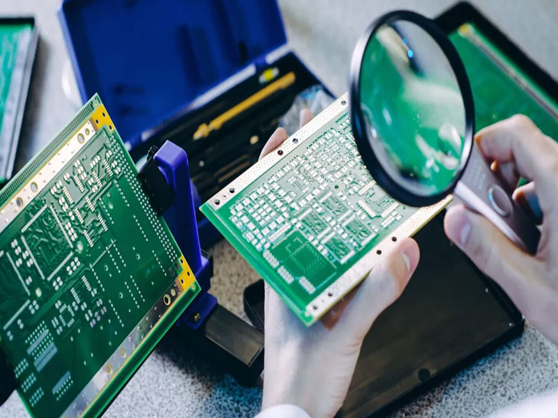
At intake the reference designators, the placement angles and the assembly drawing are checked against each other. The communication module, the antenna connector, the crystal and the polarised parts are the positions that receive the closest attention, because a reversed module or a substitute in a different package is a fault that no amount of inspection after the fact will repair.
A gateway board usually carries fine pitch devices, a shielded module and comparatively large network connectors on the same panel. The stencil is therefore evaluated part by part rather than as one pattern. After printing, SPI measures the area, the volume and the offset of the deposit, because a print problem caught before placement is a correction, while the same problem caught after reflow is a repair.
Where the customer supplies the communication module or the main processor, the original packaging and the full material information are kept together. If the material has already been opened, its storage condition is stated as well, so that the decision to release it to the line is made on evidence.
Controlling the First Article
After the first board has been printed and placed, the position and the direction of the processor, the memory, the communication module, the power devices and the interface parts are confirmed. Once the board has been reflowed, optical inspection covers the missing parts, the offset, the reversed parts and the visible joint anomalies, and a machine alarm is reviewed by a person rather than accepted on the strength of the image.
The first article of a gateway board cannot stop at appearance. Where the order includes programming and testing, the write, the read back of the revision and the basic functional verification follow as part of the same release. That is how a programming port definition, a firmware revision or an interface connection problem is found while the batch is still small.
If the same position keeps showing a soldering anomaly, the printing, the stencil, the coordinates and the reflow condition are reviewed in that order. Continuing to touch up joints one board at a time hides the cause and moves it into the volume order.

Connecting Programming to the Functional Test
Before programming, the programme revision and the board revision are checked against each other. After the write, the checksum or the version is read back by the method the customer specifies. Boards that carry individual data are held in separate flows for not yet written, written and verified, and written but failed, because a board that has been programmed with the wrong file cannot be identified later once it has been mixed into a group.
Functional test follows the customer’s method: start-up, supply, network port, communication module, indicators and buttons. When a board fails, the possibilities are the programme, the soldering, the material and the connection, and they are separated rather than guessed at. A board that has been repaired repeats the corresponding test before it is released.
In volume, different hardware and programme revisions are kept apart. Finished boards are packed in antistatic material with the antenna connector, the pin headers and the network port protected from compression, because a board damaged in transit fails in a way that looks like a design fault.
Our IoT PCBA team handles gateway boards, SMT assembly covers the placement and the inspection, component procurement looks after the module supply, and PCBA testing takes the programming and the functional check. The records are held under quality management.
Packing, Storage and Repeat Orders
A gateway board carries parts that stand proud of the surface, and those parts decide how the finished goods have to be handled. The antenna connector, the pin headers, the network port and any module with a metal shield are the first to suffer when boards are stacked without separation or when a carton is compressed. Finished boards travel in antistatic material with those areas protected, and boards are held by the edges during inspection so that a module is never used as a handle.
The record that goes with the batch is what makes a repeat order straightforward. The material lot numbers, the stencil revision, the placement programme revision, the reflow profile, the programming revision and the test result are held against the order, so the second batch can be compared with the first instead of being rebuilt from memory. When the customer issues a firmware update or changes a module, the batch from which the change applies is confirmed in writing and the superseded material is withdrawn from the line.
A new gateway design is best introduced through a small batch that verifies the artwork, the coordinates, the stencil, the programming port and the test fixture in one pass. That batch then becomes the reference for the volume orders, and every later change is measured against it rather than against a set of verbal notes.
FAQ
Why does a gateway board pass appearance and still fail? Because the direction of a module, the firmware revision and the network configuration are separate from the solder joints, and a fault in any of them shows up only when the product is powered.
Can a substitute module be used? Only after the package, the body marking and the direction of the packaging have been confirmed, because two electrically equivalent modules can present their pin one differently.
What does the first article include? The paste condition, the placement, the orientation, the joints and, where the order includes them, the programming and the basic functional verification.