Consumer Electronics Solution Development for Smart Devices
Developing a consumer electronics product is not the same exercise as developing an industrial one, even when the electronics are comparable. A consumer product is measured against a cost target that has been set by the market rather than by the bill of materials, against a schedule that has been set by a season rather than by a project plan, and against the experience of an end user who will return it if the app disconnects or the battery does not last the day. The solution development approach described here treats cost, performance and manufacturability as three constraints that have to be satisfied at the same time.
What Makes the Consumer Case Different
The first difference is sensitivity to cost. A consumer product ships in volume, so a few cents on the bill of materials multiplied by an annual quantity is a real number rather than a rounding error. The choice of the main device and its surrounding components is therefore made during the solution stage, when a cheaper route is still a decision rather than a redesign.
The second difference is the speed of iteration. Product lifecycles are short, so the work has to move from a concept to a sample, from a sample to a verified design and from a verified design into volume without long pauses. A development plan that assumes unlimited rounds does not fit the calendar.
The third difference is that user experience is a specification. The stability of the wireless connection, the charging time, the battery life and the response of the interface are the things the customer will actually notice, and they have to be measured during development rather than assumed.
The fourth difference is the volume itself. Because the quantities are large, consistency between units matters as much as the performance of any single unit, and a design that is difficult to assemble will show up as a yield problem that no amount of testing can remove.
The working principle that follows is to make the core function stable first and add features afterwards, because a product whose main function is reliable can absorb a late feature while a product built on an unstable core cannot.
The Project Flow
The work starts with a requirement assessment and a choice of technical route, in which the main device and the surrounding architecture are selected against the product’s function. A preliminary cost estimate and a development schedule are produced at the same time, because those two numbers are what a decision to start is actually based on.
The schematic and the layout follow. A consumer board is usually compact and densely routed, so the placement of the parts, the return paths and the electromagnetic behaviour are decided together rather than in sequence.
Firmware development runs beside the hardware rather than after it, covering the device drivers, the application logic, the communication protocol and the interface to the phone application, so that the first board can be brought up as soon as it returns.
Prototype verification then covers function, performance and reliability: the temperature extremes, the aging behaviour and the battery runtime. Two or three rounds are normal before the design is frozen, and the findings from each round are folded into the next revision rather than collected into a report.
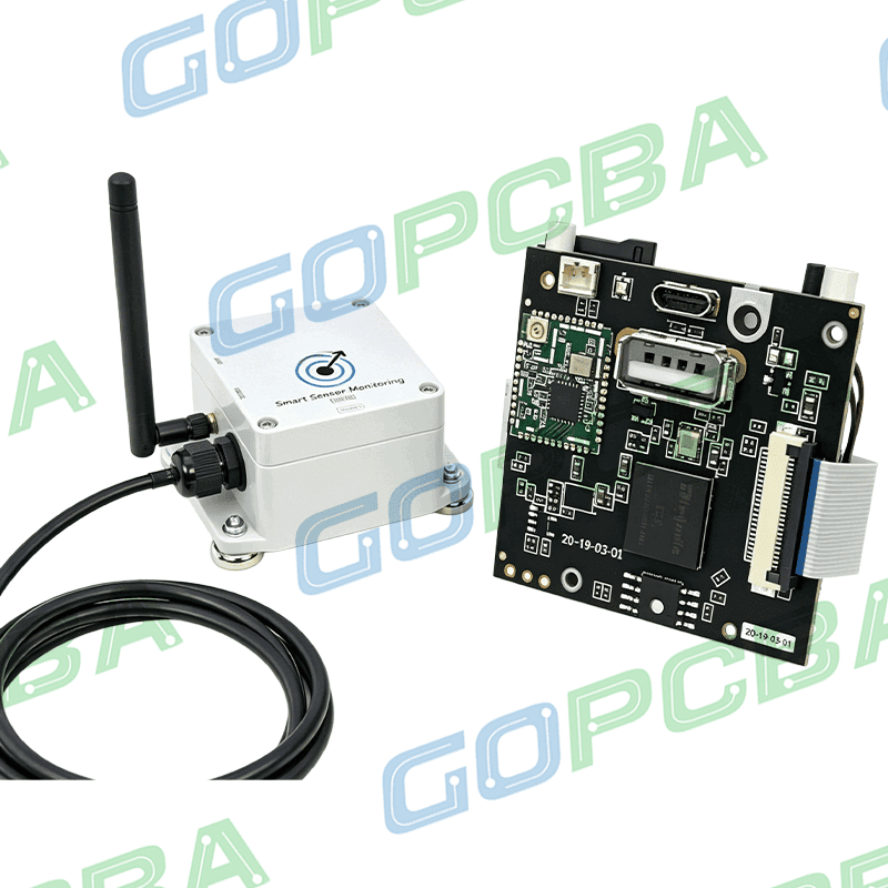
A pilot production run closes the loop. Its purpose is to prove the process rather than the design: the stencil, the placement programme, the reflow profile and the test fixture are exercised on a real batch, and the issues that only appear at volume are found while the quantity is still small. After that the order moves into regular production on our own assembly lines.
<img src="https://www.gopcba.com/wp-content/uploads/2026/08/PCB-1.jpg" alt="pilot production batch of consumer electronic boards” />
Two Project Examples
The first is a household temperature and humidity monitor with a display and a wireless data link. The requirement was a small enclosure, a long battery life and an accurate reading, and the development focused on the sleep strategy of the processor and the sampling interval of the sensor, together with a calibration routine that corrects the sensor across the range in which the product is used.
The second is a control board for a small kitchen appliance, with touch keys, a display, several operating levels and protective functions. The cost pressure on that board is severe while the safety and electromagnetic requirements cannot be relaxed, so the component selection and the board layout were optimised inside the target cost and the compliance work was started early. The production yield after release held above the target.
How the Work Is Structured
The advantage of a single supplier from the concept to the shipped board is that nothing is lost at a handover. The people who selected the components see the boards being assembled, and the people who run the line were consulted while the layout was still open. Cost work uses the component database and the qualified alternatives that component procurement maintains, so a cost reduction is a qualified substitution rather than an untested swap.
The commercial arrangement is flexible. A customer can hand over the whole requirement and receive a production ready design, or keep the software team and take only the hardware work, or divide the development between two teams by discipline. An existing design can also be modified for a new variant, which shortens the schedule and lowers the cost. Our PCB design and layout group, the embedded firmware team and the SMT assembly lines sit inside the same company, and the records are held under quality management.
Where Cost Optimization Actually Happens
Cost optimization on a consumer product is not a negotiation held at the end of the project. It is a series of decisions taken while each one is still reversible, and the later a decision is taken the more it costs to make. The first opportunity is the architecture: the choice between a single integrated device and a processor with separate peripherals can move the bill of materials by more than any individual component negotiation, and it is settled before the schematic is drawn.
The second opportunity is the component selection. Every part that carries a meaningful cost is compared against a qualified alternative from the component database, with the package, the temperature range and the availability considered alongside the price, so that the saving does not create a supply problem or an assembly problem later.
The third opportunity is the board itself. The layer count, the panel utilisation and the finish all carry cost, and a layout that fits a smaller panel or avoids an unnecessary layer reduces the price of every unit without changing the function.
The fourth opportunity is the assembly. A footprint that prints and places cleanly produces a higher yield than one that does not, and yield is a cost that appears in the production figures rather than in the quotation. A part that is half a cent cheaper but adds two percent to the defect rate is not a saving at all.
The whole exercise is bounded by the specification. Features that the user will notice are not traded away for cost, and the safety and electromagnetic requirements are treated as fixed. What remains is a design in which the cost has been removed from the places where it buys the least, which is a different activity from making the product cheaper.
FAQ
Is the cheapest solution the objective? No. The objective is the best core experience at the cost the market allows, which is why the trade-offs are made during the solution stage rather than by downgrading parts afterwards.
How many prototype rounds are usual? Two or three for a consumer product, with the findings of each round folded into the next revision.
Why run a pilot batch before volume? Because the problems that appear at volume are process problems, and the pilot run is the cheapest place to find them.