Communications PCBA: Shielding and Interface Testing
Communications equipment is judged by whether the link stays up. The board may be small, the component count modest and the assembly unremarkable, and the product will still be judged in the field on signal stability, interface reliability and the behaviour of the unit after months of operation. That is what makes shielding and testing the two subjects that determine whether an assembly programme succeeds.
The boards carry a controller, memory, a network interface, an RF module, a crystal, power management, a shield can, connectors, an antenna connection, an Ethernet port and a USB interface. They are densely populated, several of the devices are static sensitive, and the population includes parts whose correct position matters mechanically as much as electrically.
Critical Devices and Their Versions
Communications products carry modules with revisions, devices with suffixes, crystals with specific frequencies and connectors and shields with defined dimensions. A bill of materials that does not state these precisely cannot be purchased accurately, and a substitution that has not been assessed can produce an unstable link, an abnormal current draw, an incompatible interface or a mechanical clash.
The decisive question for a substitute is not whether it can be purchased but whether it suits the design. A module that is electrically equivalent but a millimetre taller may not fit the shield; a crystal with the same nominal frequency but a different load capacitance may not start reliably; a connector with the same pin count but a different latch may not mate with the cable the customer uses.
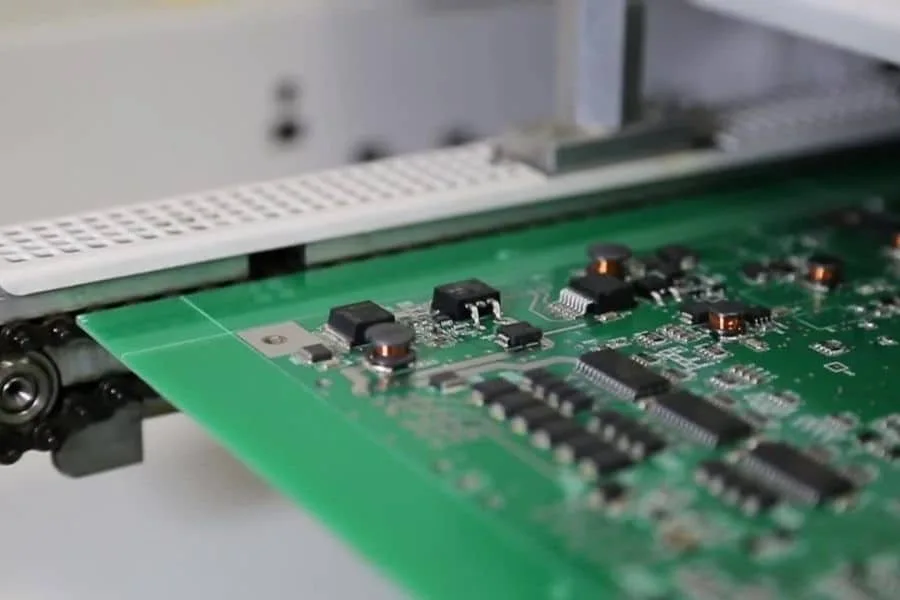
<img src="https://www.gopcba.com/wp-content/uploads/2026/08/Three-Main-Circuit-Board-Components.jpg" alt="communications PCBA with shield can and RF connector fitted” />
Placement and the Parts That Must Sit Square
The boards carry fine pitch devices, QFN and BGA packages, small passives and high density connectors, so paste printing, placement accuracy and the reflow profile all determine whether the joints are reliable. The RF connector, the network port and the shield footprint add a mechanical requirement on top of the electrical one, because their position and squareness decide whether the cable, the plug or the shield will engage properly.
Those parts are confirmed on the first article with the same attention that a fine pitch device receives. A connector soldered a fraction of a millimetre out of position still conducts and can still refuse to accept its plug, and the resulting complaint will describe a product that does not work rather than a joint that was misplaced.
Fitting the Shield
A shield can is fitted to reduce interference or to meet a product requirement, and it depends on the assembly as much as on the design. The pads, the grounding points, the height of the components beneath it, the clearance to the enclosure and the possibility of removing it for repair all have to be consistent.
A can that is distorted, seated unevenly or soldered with gaps in its ground connection does not shield as intended, and the symptom is a product that behaves differently from the prototype in a way that is difficult to attribute. Where the shield has to be removable, the method of fixing it is agreed before production rather than decided at the bench, because a shield that has been soldered in place and then removed has usually damaged the pads it was soldered to.
Programming and Configuration
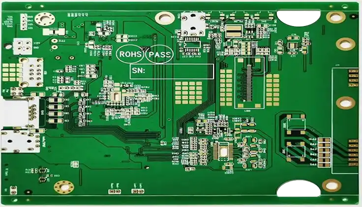
Soldering completes the hardware and the product is not usable until the firmware and the configuration are in place. The files, the method, the version description and the rules for unique data are supplied with the order: whether a serial number or a MAC address is written, and how the values are generated and prevented from repeating.
Multiple programme versions, different configuration parameters and different identifiers can exist on the same board design, and they are indistinguishable to an operator. The version and the configuration are therefore carried by a label, a tray position or a record, and the distinction is made before the boards are packed rather than after they have been delivered.
Standardising the Communication Test
The test items for this class of product are predictable: the switch-on current, the programme, the network or serial communication, the wireless module connection, the indication states, the interface recognition and the power consumption. What varies is how rigorously they are performed.
Manual testing is acceptable for a prototype, but a test fixture or at least a fixed procedure becomes necessary as the quantity rises, because the reliability of a communications interface cannot be judged by watching it for a few seconds with different cables on different benches. The fixture does not have to be elaborate; it has to make contact reliably, produce a clear pass or fail, and produce a record that can be compared with the last batch.
Where the customer supplies the fixture, it is delivered and proved before the batch is scheduled. Where the assembly supplies it, the interface definition and the test sequence come from the customer, because the acceptance criterion belongs to the product.
Packing for Parts That Protrude
Communications boards carry shields, antenna connections, ports and connectors that sit above the board surface, and those are the features that take the load when a carton is compressed. Antistatic bags, trays, foam that separates the boards and labels that allow a batch to be identified without opening the packing all reduce the damage that appears between the factory and the customer’s line.
Where the boards are destined for a unit assembly, packing by version, batch or project is worth agreeing in advance, so that the boards arrive in the groupings in which they will be consumed.
The work is carried out as SMT assembly, with the verification through PCBA testing, the material through component procurement, the unit assembly that follows through box build assembly, the criteria under quality management and the product context under telecommunications PCBA.
Where Communication Problems Are Actually Found
A communication fault is rarely caused by the device an engineer first suspects. It is found by elimination, and the elimination goes faster when the assembly record exists. A link that drops under load, an interface recognised intermittently or a module drawing more current than expected can come from a joint, a component, the programme or the design, and the order in which those are eliminated decides how long the search takes.
Starting from the assembly is usually cheapest, because the record is already there: the board revision, the programme version, the material lots and the test results. With those known, comparing batches immediately shows whether the problem is confined to one delivery or appears in several, which by itself separates a material or process question from a design question.
It also helps to keep the test evidence rather than only the verdict. The current drawn at switch-on, the state of the indicators and the outcome of the interface test are the figures that place a fault in time, and a note recording that a board passed tells nobody what it actually did.
FAQ
Why does the shield affect the result? Because it only works when it is level, properly seated and connected to ground across its full perimeter; a partial connection changes the behaviour of the product.
Can a communications module be replaced by an equivalent? Only after the revision, band, firmware and dimensions have been assessed, since these determine both the radio behaviour and whether the module fits.
Why standardise the test early? Because the stability of a communications interface cannot be judged by eye, and a test that is not repeatable cannot be compared between batches.