PCB Tooling Hole Position on the Panel: Locating the Panel
Buyers and engineers often focus on the finished product and forget the production line behind it. In practice, most field failures can be traced back to process decisions made during assembly. Understanding PCB tooling hole position on the panel gives you a practical advantage when you choose a factory, review a quotation or troubleshoot a quality problem, because it shows exactly where positioning the holes that hold the panel can go right or wrong.
1. What PCB Tooling Hole Position on the Panel Means in Practice
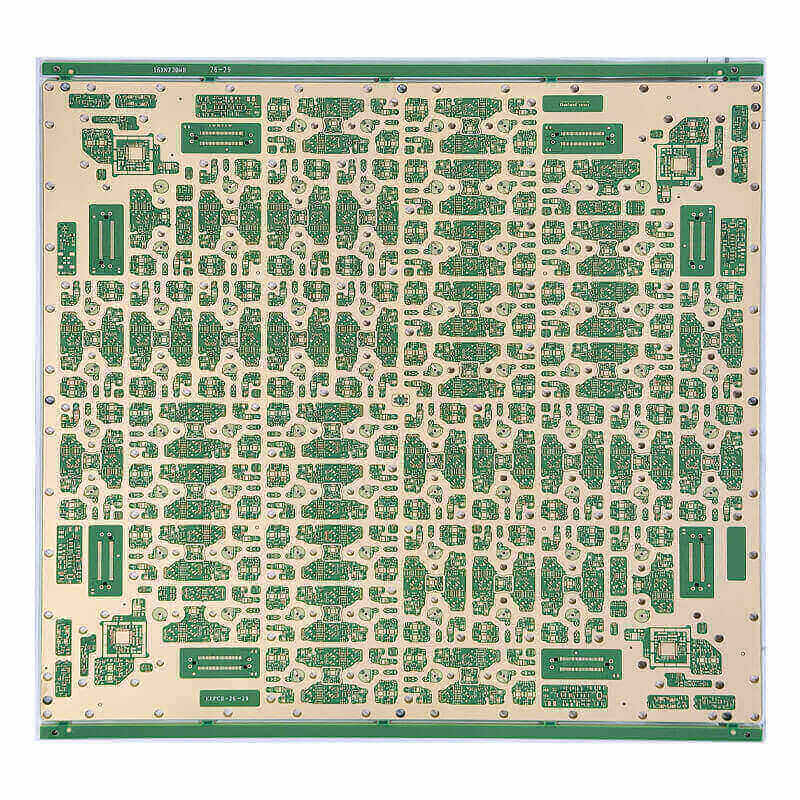
Where the holes go and how much clearance they need.
2. The Production Route in Practice
The result depends on the whole chain, not on any single machine. The board design fixes pad sizes and spacing, the printer controls the solder volume, the placement machine positions every component and the reflow oven forms the joints. Each step feeds the next one, which is why SMT PCB assembly should be reviewed as one complete process instead of a collection of separate operations.
3. Why It Matters
A hole that clashes with the array wastes panel area on every order.
4. Checks That Hold the Yield Steady
First article inspection plays a special role at the start of every order. The first board is checked against the design in detail: component values, orientation, polarity and solder quality are verified before the line continues, which prevents an entire batch from inheriting a setup error. After the run, every board passes automated optical inspection, and samples move on to electrical test so the solder joints and the circuit are both proven before packing; this combination is the core of a practical PCBA testing plan.
Traceability turns good intentions into proof. The factory records which program ran, which reels of paste and components were used, which operator handled the job and what the inspection found. When a field return arrives six months later, that record is the fastest way to find the cause, and it is the clearest evidence that a documented quality management system is working.
5. Where These Boards Are Used
Assembled boards built with a well controlled process serve every industry: PCB manufacturing, panel and tooling. The same core disciplines apply across all of them, but each market adds its own expectations. Consumer products need low cost and fast ramp, medical products demand documentation and traceability, automotive boards must survive vibration and temperature extremes, and industrial electronics value long service life and easy repair.
6. Designing It
The holes are placed with the machine pins and the array in the same drawing.
7. Choosing the Right Manufacturing Partner
Most boards today are built by specialists rather than in house. The investment in printers, placement machines, reflow ovens and inspection equipment is large, and the engineering time needed to keep the process stable is easy to underestimate. A manufacturing partner spreads that cost over many programs and brings the same discipline to every customer, with supporting services such as mixed technology PCB assembly available from a single source.
The choice between suppliers comes down to behavior under pressure: how a factory reacts to a design question, a component shortage or a quality issue tells more than its brochure. Ask for defect data, test coverage and customer references, and confirm the quality plan in writing before you commit a program.
8. Details That Are Easy to Overlook
Collecting data about positioning the holes that hold the panel pays for itself quickly. Print reports, placement statistics, oven profiles and test results cost little to record, yet they turn arguments into decisions: when a customer complains, the batch record shows what actually happened, and when a process drifts, the trend line reveals it before scrap grows. Factories that treat records as part of the process rather than paperwork tend to find problems while they are still cheap to fix, and their customers see the difference in delivery performance and defect rates over time.
9. Working With gopcb on Your Project
We treat pin as a shared target: the DFM review, the production run and the final report all check against it, which keeps a repeatable result across batches.
At gopcb, process control is a habit rather than an exception. Every batch is printed, placed and reflowed against a written specification, inspected at the right stages and tested before packing. Our engineers speak the same language as your design team, so questions about pads, profiles and tolerances are answered quickly.
Contact gopcb with your design files today. We will confirm the manufacturability of your board, recommend the right assembly route and deliver quality boards on the schedule your product launch needs.
Prototypes are the cheapest place to make mistakes, and early samples teach more about positioning the holes that hold the panel than any quotation does. The first small batch reveals pad geometry problems, component tolerances and process behavior before thousands of boards are committed, so the DFM review and the pilot run should be treated as part of the project rather than as an extra expense. Buyers who invest in this stage almost always reach volume production faster and with fewer surprises than those who rush straight to the big order.
There is more to positioning the holes that hold the panel than the machines and materials visible on a factory tour. Temperature and humidity in the assembly area change the behavior of solder paste, and electrostatic discharge can damage sensitive components without leaving a visible mark. Professional factories control these conditions, ground every workstation and store moisture sensitive devices correctly, so the process produces the same result in summer and in winter. These environmental details rarely appear in a quotation, yet they decide whether a line runs at high yield all year or drifts with the seasons.
Documentation matters as much as hardware when it comes to positioning the holes that hold the panel. The factory should record which program ran, which reels of paste and components were used, which operator handled the batch and what the inspection found. When a field return arrives months later, that record is the fastest way to identify the cause and to prove that the fix reached the next batch. Buyers should ask for these records as a routine part of every order, because documents that are easy to produce on request are usually also kept honestly during production.
Nothing about positioning the holes that hold the panel is decided once and forgotten. Parameters drift, materials change and operators rotate, so the factory reviews its data continuously, ranks the top defects and removes them one by one. Factories that follow this discipline gradually lower their defect rates and shorten their lead times, while factories without data simply repeat the same mistakes at the same cost. The improvement review should happen at least monthly, with the same attendees and the same metrics, so progress stays visible and no problem waits for a crisis to be fixed.
Conclusion
To sum up, PCB Tooling Hole Position on the Panel is decided long before the final inspection. The design data, the material, the setup and the in process checks each hold a share of the result, and a factory that treats them as one chain produces boards that behave in the field exactly as they did on the line. Buyers who ask for the drawings, the settings and the test records usually find that positioning the holes that hold the panel turns into a predictable part of the schedule instead of a risk to it.
That covers everything in “PCB Tooling Hole Position on the Panel: Locating the Panel”. If you need layout design, PCB fabrication, SMT assembly, component sourcing, stencil making, conformal coating, box build or functional testing, our engineering team can review your files and quote the work. Send your design data to gopcb and we will return a manufacturability review, a clear price and a firm delivery date.