Power Bank PCB Design: Components, Layout, Protection
A power bank is a battery, an enclosure, and a small circuit board that decides whether the product is safe, efficient, and durable. That board manages power distribution, regulates voltage, protects the cell, and handles the interfaces the user touches. Designing it well is mostly about two things: keeping the switching path short and keeping heat out of the cell.
What the board does
The board sits between the battery and the outside world and performs three functions. It distributes power between the cell, the input connector, and the output ports. It regulates voltage, converting the cell voltage into a stable output for the device being charged and a controlled charging profile for the cell itself. And it protects the cell and the user, which is the function that determines whether a product can be sold at all.
Those three functions are performed by four blocks, and reviewing them separately is the fastest way to check a design.
Battery management system
The battery management system regulates charging and discharging and prevents overcharge and overheating. It defines the charge profile, monitors the cell voltage and temperature, and terminates the charge when the cell is full. On a single-cell product the function is compact, but it is not optional: a cell charged without a defined termination criterion is a safety risk rather than a design weakness.
Voltage regulation and conversion
A single lithium cell delivers roughly 3.7 V nominal, while the output is usually 5 V for a USB load. The conversion is performed by a boost converter, and its efficiency curve decides how much of the stored energy reaches the load and how much becomes heat inside the enclosure.
Efficiency is the parameter that matters most in this block. A converter that is efficient at the rated load but inefficient at the standby current wastes energy continuously, and a converter with poor light-load behaviour turns a large part of the stored energy into heat on a small board.
Protection circuit
The protection block covers overcurrent, overvoltage, short circuit, and over temperature, and it is typically implemented by a dedicated protection device in series with the cell, backed up by the converter and the management logic. The acceptance criteria are set by the certification the product must pass, not by the designer preference.
Interfaces
The input charging connector and the output ports complete the design, together with the sense circuitry that reports charge state to the user. Connector placement is a mechanical decision as much as an electrical one, because the ports carry the full output current and their position sets the length of the high-current paths on the board.
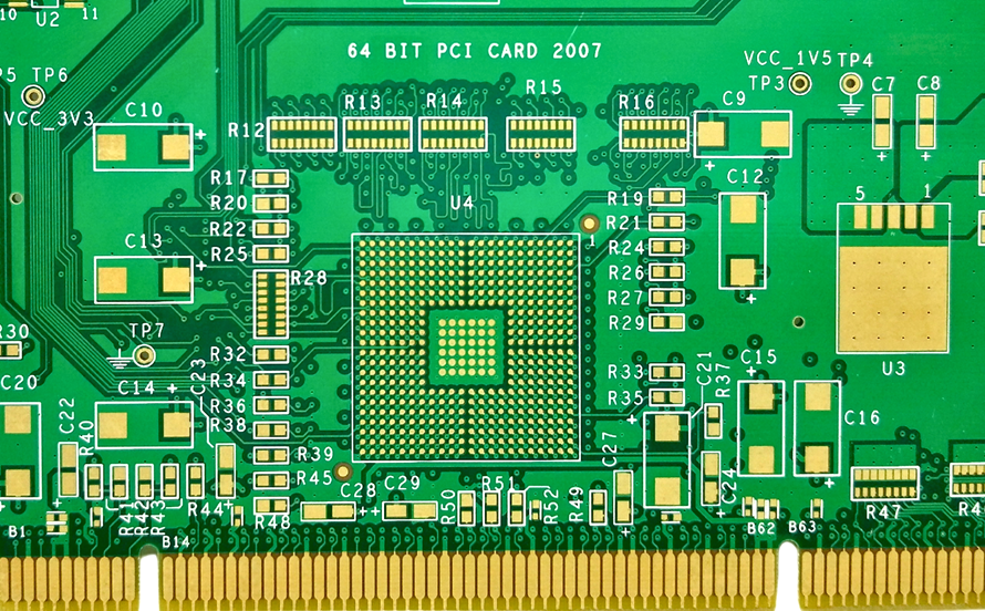
The high-current loop from cell to converter to connector should be short, wide, and continuous on the board, because every millimetre of that path adds resistance and heat.
How the power path works
Discharging converts the cell voltage up to the output voltage; charging converts the input voltage down to the cell. Both directions pass through the same switching stage, and in both directions the losses appear as heat in the inductor, the switching device, and the copper.
That heat has a consequence beyond efficiency. A cell that is warmed by its own electronics ages faster and, in the worst case, becomes unsafe. Thermal design on a power bank board is therefore a safety measure, not a comfort feature, which is why the layout rules for switching converters matter here more than they would on a signal board. The relevant geometry is covered in our guide to DC to DC converter layout and routing.
Board types
Layer count is the first choice. A multilayer board improves performance and spreads heat better than a single-sided one, because the additional copper helps distribute the thermal load away from the switching devices. Flexible substrates are used where the board must follow the shape of a slim enclosure, while rigid boards remain the default for durability and cost.
The second choice is between a standard design and one built around efficiency. An advanced power management design with a well-chosen converter and a clean layout extends the energy a user gets from the same cell, which is a product feature rather than a technical detail.
Design factors
Material selection sets the ceiling on thermal performance. FR-4 is adequate for lower-power designs, an aluminium substrate moves heat far more effectively, and high-performance composites occupy the space between them. The choice should follow the measured dissipation rather than the habit.
Layout and thermal management go together. The switching loop, the sense connections, and the thermal relief around the converter determine both the electrical behaviour and the temperature rise. Component placement then decides how well the design tolerates the heat it produces: keep the cell away from the converter, keep the sense resistor in the coolest available area, and give the inductor enough copper to work with.
Copper width is not a detail to settle at the end. The cell, the inductor, and the output connector form a high-current path, and its width should be calculated from the current rather than estimated. The method is described in our guide to trace width and current calculation.
Manufacturing
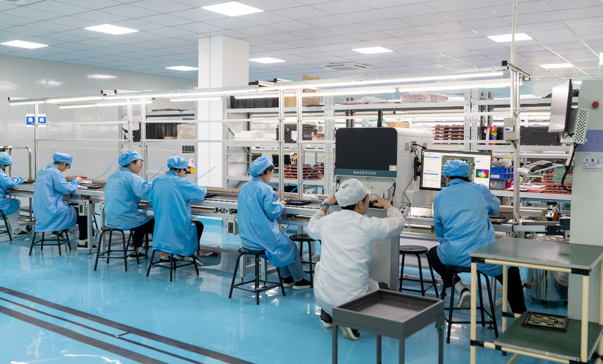
Fabrication follows the standard sequence: stackup, etching, and drilling create the circuit paths, and assembly places components using surface mount technology for the fine parts and through-hole technology for connectors that must withstand mechanical load. The reflow conditions depend on the alloy chosen, and the differences are set out in our guide to lead-free versus leaded solder.
Test and certification come last and should be planned first, because they define what the design has to achieve. A portable charger typically needs to demonstrate compliance with the applicable safety, chemical, and electromagnetic requirements, and each of those translates into a design constraint: creepage distance, temperature limits, and emission behaviour.
Certification is cheaper to pass when the layout was designed for it. Retrofitting clearance and thermal margin after the first prototype costs a board revision.
Common problems and how to avoid them
Overheating is the most common complaint, and it usually traces back to inadequate thermal design rather than to a component failure. More copper, a shorter high-current loop, and a converter with better efficiency at the actual load all reduce it.
Low charging efficiency is the second, and it is visible in the heat produced for a given output. A converter chosen for its efficiency curve rather than its headline rating, combined with a layout that keeps the switching node small, addresses most of the loss. Board failure, the third, is usually a component quality issue, and it is the reason a sample build and screening are worth the time.
Sourcing notes
Price follows the same variables as any board: material quality, layer count, order quantity, and customisation. A design that needs an aluminium substrate or a higher layer count costs more than a simple two-layer FR-4 board, and a custom shape or an unusual connector adds tooling and handling cost.
When evaluating a supplier, four questions are worth asking. Which quality systems and certifications apply to the process? Can a sample build be inspected before a production order? What is the manufacturing lead time at the planned quantity? And what is the minimum order quantity, since that decides whether a small pilot build is possible at all. Logistics then completes the calculation, because shipping cost and import compliance are part of the total even when the board price is low.
Power bank PCB design is a compact exercise in power electronics: a short high-current loop, a converter whose efficiency matches the load profile, a protection block that satisfies the certification, and a thermal path that keeps the cell cool. Each of those is a layout decision as much as a component decision.
FAQ
What is the most important part of a power bank PCB? The battery management system, because it defines the charging behaviour and the safety limits. A high-efficiency converter is worthless if the cell is charged outside its specification.
Do I need a multilayer board? Not for a basic product. A multilayer board becomes worthwhile when the thermal load rises or when the switching loop cannot be kept short on a single layer.
How do I reduce heat without changing the components? By shortening and widening the high-current paths, keeping the switching node small, and increasing copper area near the converter. Layout changes cost nothing per unit and often outperform a component upgrade.