Switching Regulator PCB Layout: Loops, Grounding and Checks
A switching regulator is a small circuit with a large appetite for current, and the layout decides whether that current stays where it was planned or sprays across the board. The electrical design can be textbook correct and the prototype still fail, because the paths that carry the switching current have inductance, and every millimetre of that inductance converts into ringing, radiation and loss.
The Four Current Loops in Every Converter
Every switching converter contains four current paths: the input source loop, the power switch and rectifier commutation loop, the output rectifier loop and the output load loop. The first and last carry roughly DC currents and are comparatively forgiving. The middle two carry trapezoidal currents with rise times near 50 ns and peak amplitudes several times the DC output current, and those are the paths that have to be laid out before anything else on the board is placed.
Treat the commutation loop as the primary constraint. The input capacitor, the switch and the rectifier or synchronous device form a single closed path, and the area of that path sets both the radiated field and the overshoot at the switch node. Once the loop is placed, the rest of the layout follows.
Placement Order
A workable order is to place the transformer or inductor first, then build the switch loop around it, then the rectifier loop, then the control circuitry that connects to the switching stage. The input filter and the input source loop come next, and the output filter and load loop last. This order is not arbitrary: it places the components whose position is fixed by the current paths before the components whose position is flexible.
Keeping the filter capacitor, the switch and the rectifier adjacent to one another is what makes the loop small. Adjusting the position of a transformer by a few millimetres to shorten a commutation path is almost always a better trade than routing around it.
<img src="https://www.gopcba.com/wp-content/uploads/2026/05/病人监护仪-PCBA.png" alt="Switching regulator layout showing a compact commutation current loop” />
Input and Output Capacitor Terminals
The terminals of the input and output capacitors are the anchors of the two quiet loops. Current should flow from the capacitor terminal to the switching stage and back, without sharing a section of copper with anything else. When the input loop and the switching loop have to share a trace, the shared impedance radiates the trapezoidal current into the environment and couples it into the control circuitry.
Because the capacitor is the anchor, its placement is a layout decision rather than a schematic decision. Two capacitors in parallel, one ceramic close to the switch and one bulk part nearby, usually outperform a single larger capacitor placed further away.
Trace Width and Impedance
The inductance of a trace is proportional to its length and only weakly dependent on its width, while the resistance falls with width. That asymmetry is why short matters more than wide for high-frequency paths, and why both matter for the DC paths. Route every conductor that carries alternating current as short and as wide as the space allows, and connect the associated components with the shortest possible links.
A trace that carries only DC is not automatically safe. It can couple energy from a nearby switching trace, re-radiate it, and create a problem in a circuit that has no switching current of its own. Separation and a ground reference are the tools for that case.
Grounding Strategy
Ground is the common return of all four loops, which is exactly why mixing ground types causes instability. In a converter of modest complexity, single-point grounding works well: the return of the input capacitor, the switch, the rectifier and the output capacitor all meet at one place, usually the ground terminal of the filtering capacitor. The reference potential of each stage then stays tied to a single point and the circulating current through shared copper is minimised.
Where a genuine single point is impractical, a compact area of copper that several returns share is the next best option. The objective is the same either way: keep the impedance that the return current sees as low and as local as possible.
Making the Ground Wide Enough
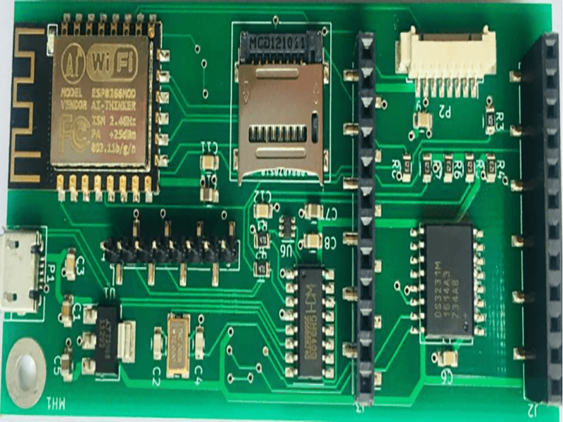
Ground traces should be wider than power traces, and power traces wider than signal traces. For a converter carrying meaningful current, a ground conductor in excess of 3 mm is a sensible starting point, and unused board area is better filled with ground than left bare. A thin ground trace develops a voltage that varies with the switching current, which modulates the reference of the timing and control circuits and shows up as jitter or instability.
Widening the ground also lowers the impedance that the commutation loop sees on its return leg, which directly reduces the overshoot at the switch node.
Routing the Control Section
The control circuitry needs a quiet reference. Place the controller away from the switching node, keep the feedback divider connection to the output sense point short and direct, and route the compensation network so it does not run alongside the switch node or the rectifier. The feedback connection should be taken from the output capacitor terminal rather than from an arbitrary point on the output copper, because that terminal is the point where the output is actually quiet.
Where the converter drives a low-voltage output from an isolated input, the input and output grounds eventually have to be connected to give the feedback path a common reference. Copper each side separately first, then join the two areas at a single defined point rather than allowing them to merge along a broad edge.
Spacing and Electrical Clearance
Spacing is a safety parameter as well as a layout parameter. The conductor spacing has to satisfy the electrical safety requirement for the working voltage, and the minimum spacing should still be comfortable for production. In low-density areas the spacing can be increased at no cost. High and low level signals should be routed short and separated, and the hole edge of any pad should stay more than a millimetre from the board outline to prevent edge damage during fabrication.
Where a thin trace meets a pad, a teardrop transition improves the mechanical strength of the joint, which matters for a converter that will be thermally cycled.
Checking the Design Before Release
After routing, re-run the rules rather than trusting the layout to be self-consistent. Check conductor to conductor spacing, conductor to pad spacing, pad to via spacing and via to via spacing, and confirm that the power and ground widths are as intended. If the stack-up changed, or if vias were added late, re-pour the copper before generating the outputs, because the fill and the connectivity check depend on the final geometry.
The manufacturing outputs themselves deserve a check: routing layers, silkscreen on both sides, solder mask on both sides, the drill layer and the numeric control drill file. Our design release checklist covers the review sequence, the thermal management material covers the heat path that a converter depends on, and the component tolerance and reliability notes explain why a marginally rated part is the one that fails first. Designers working on converters that feed radio or high-speed sections should also read our EMI immunity design notes.
FAQ
Why does the switching node ring even though the schematic is correct? The ringing is produced by the commutation path, specifically the loop area and the equivalent series inductance of the components in it. Reducing the physical size of the loop, using a capacitor with lower equivalent series inductance and keeping the switch and rectifier adjacent are the measures that reduce it. Changing the schematic rarely helps, because the parasitic elements that cause the ringing are not in the schematic at all.
Is single-point grounding always required? It is the clearest approach for a converter with a modest number of stages and it is what most switching designs should start with. Where the currents are large or the number of stages makes a literal single point impractical, a compact common copper area that the returns share gives most of the benefit, provided the area is small and the connections to it are short and wide.
What does gopcb recommend before generating manufacturing data? Re-run the spacing and width rules after the final copper pour, then verify that the silkscreen, solder mask and drill outputs match the released stack-up. Most converter problems we see in fabrication review are not electrical design errors at all; they are spacing or fill issues introduced by a late edit that was applied to the routing but not re-checked against the fabrication rules.