PCB Layout Planning: Structure, Placement and Routing Strategy
Layout is where a correct schematic either becomes a working product or a source of problems that no amount of firmware work will fix. Most of that outcome is decided before the first track is drawn, in the decisions about board structure, functional partitioning and placement. Planning those properly is what separates a design that routes easily from one that requires repeated rework.
Why Planning Beats Rework
Experienced designers spend more time on optimisation than on the initial routing, often twice as much. That figure is not a measure of indecision; it reflects the fact that a layout reviewed after completion almost always reveals improvements. A problem found during planning costs a decision, while the same problem found after routing costs the work of rerouting around it.
In PCB layout planning the practical consequence is that the sequence matters. Structure first, then placement, then routing, then optimisation, with verification at each stage. Skipping ahead to routing before the mechanical constraints and the functional zones are settled produces layouts that have to be redone.
Structural Design Before Any Layout
The first step is mechanical. Using the confirmed board dimensions and the mechanical fixing points, the board outline is drawn and the parts that interface with the outside world are positioned: connectors, buttons and switches, screw holes and assembly holes. Their positions are usually not negotiable, because they are set by the enclosure.
The same step defines where routing is permitted and where it is not. A keep-out area around a screw hole, for example, exists because a tool or a fastener must reach that point without damaging conductors or components. Establishing these areas at the start prevents the situation where a completed layout has to be rearranged because a fixing was forgotten.
Partitioning: Digital, Analogue and Power
Layout then divides the board by electrical function. Digital circuitry forms one region, and it is both susceptible to interference and a generator of it. Analogue circuitry forms another, and its defining characteristic is susceptibility. Power drive circuitry forms a third, and it is primarily a noise source.

Once the regions exist, the rule is to keep the components of one function close together and to arrange the regions so that the connections between them are short and direct. Adjusting the relative position of whole blocks is far easier than adjusting individual components later, and it is where most of the routing difficulty is removed.
Placement Rules That Prevent Rework
Within each region, several rules apply consistently. Components that are physically heavy need a mounting position that supports them and enough board strength beneath. Heat generating parts must be separated from temperature sensitive ones, and where that is impossible the design should include provision for convection. Input and output driver devices belong near the board edge and near their connectors.
The clock source should sit close to the devices that use its output, and every integrated circuit needs a decoupling capacitor between its supply pin and ground, preferably a high frequency ceramic type. Where space is tight, a single tantalum capacitor can serve several devices. A relay coil needs a flyback diode across it, for which an ordinary signal diode is usually sufficient. Finally, placement should be balanced and orderly; identical parts aligned in the same orientation make assembly, inspection and repair substantially easier. Placement practice is discussed in placement order and pad positioning.
Routing Order and the Three Levels of Quality
Routing quality is often described in three levels. The first is simply completing the connections, with no unrouted nets remaining. The second is satisfying electrical performance, which is what actually determines whether the board behaves. The third is visual order, which matters because a layout that is difficult to read is difficult to test and to repair.
In practice routing begins with power and ground, because they define the structure that the signal layers must respect. Ground should be the widest, then power, then signals. Typical signal widths fall between 0.2 and 0.3 millimetres, with fine work reaching 0.05 to 0.07 millimetres, while power traces conventionally run from 1.2 to 2.5 millimetres. On digital boards a wide ground grid can form a useful return network, though the same approach is not appropriate for analogue grounds.
Widths, Clearances and Via Dimensions
Process requirements narrow the choices. A common starting point is a 0.3 millimetre signal trace and a power trace of 0.77 or 1.27 millimetres, with spacing between traces and pads of at least 0.33 millimetres and preferably more where space allows. Dense areas may permit two traces between integrated circuit pads at 0.254 millimetres width and spacing, but this is a compromise rather than a target.
Pads and vias follow similar conventions. A pad diameter should exceed its hole diameter by more than 0.6 millimetres; typical through-hole parts use 1.6 millimetres over 0.8 millimetres, and larger parts such as headers use 1.8 over 1.0. Component lead holes should be 0.2 to 0.4 millimetres larger than the actual lead. Vias are commonly 1.27 over 0.7 millimetres, reduced to 1.0 over 0.6 in dense designs but not below. Clearances between pads, vias, tracks and each other are normally held at 0.3 millimetres, or 0.254 millimetres in dense work. Pad geometry is covered in PCB pad design standards.
Copper Pour, Silkscreen and Optimisation
Once the layout is believed complete, copper is poured into the remaining areas, normally connected to ground, with analogue and digital grounds kept separate. Multilayer boards may also pour power. Silkscreen then receives attention: legend must not be hidden under components or removed by pads and vias, and text on the underside should be mirrored so that it reads correctly when the board is viewed from that side.

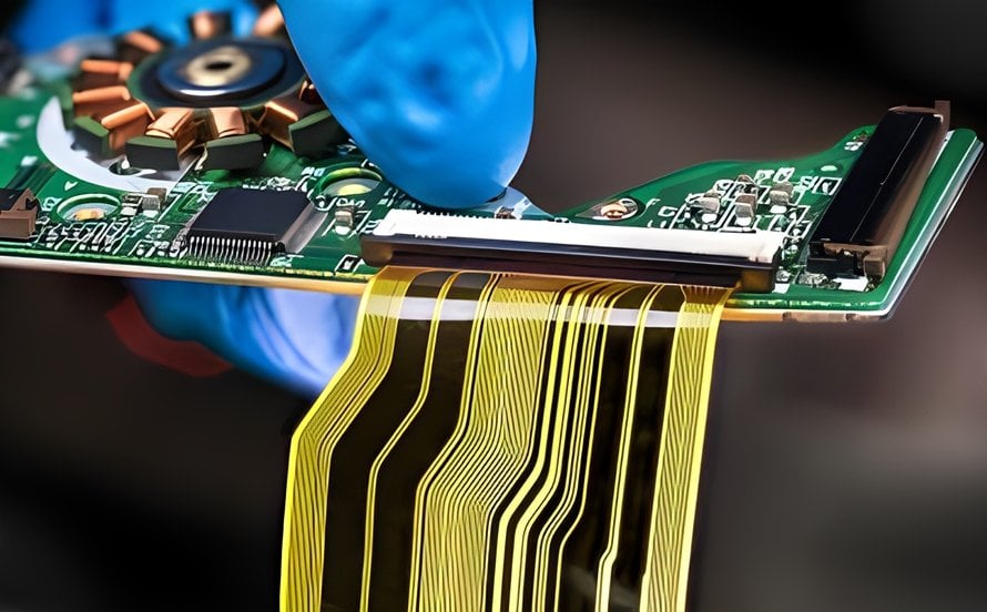
Specific routing care belongs to the same stage. Critical nets such as high frequency lines are routed first; input and output traces at the board edge should not run parallel to one another, and where they must, a ground trace between them reduces reflection coupling. Routing on adjacent layers should run perpendicular rather than parallel, since parallel traces on neighbouring layers couple more strongly than neighbours on the same layer. Oscillator cans are grounded, clock traces are kept short, and the area beneath an oscillator or high speed logic carries a large ground area with no other signals. Bends use forty five degrees rather than ninety, loops are avoided or minimised, and vias on signal lines are kept to a minimum. Critical traces are short, wide and flanked by guard ground, and sensitive signals leaving the board over a flat cable use a ground-signal-ground arrangement. EMI control is described in EMI suppression design principles.
Net Check, Design Rule Check and Mechanical Review
Verification closes the process. Assuming the schematic is correct, the board netlist is compared against the schematic netlist to confirm that the physical connections match the intended ones, and any discrepancy is corrected. With connectivity confirmed, a design rule check verifies electrical and manufacturing constraints such as clearance, width and annular ring, and its findings are resolved before release.
The final step is mechanical. Mounting positions, connector heights, component clearances and the board outline are checked against the enclosure drawing rather than against the layout alone. Test points reserved on critical signals make production and field diagnosis easier, and a formal review before release catches what the checks cannot express. The review sequence is described in PCB design review process.
FAQ
Why route power and ground before signals? Because they define the structure the signal layers must respect. Routing signals first usually forces the power network into whatever space is left, which degrades both current capacity and the return path.
How much time should optimisation take? A common rule of thumb is twice as long as the initial routing. The figure reflects how much can still be improved once the layout is complete and can be reviewed as a whole.
Is a design rule check enough before release? No. It verifies measurable constraints but cannot judge whether a placement decision makes assembly difficult or a clock trace unnecessarily long. Mechanical review and human inspection remain necessary.