LoRa Module PCB Integration: Space, SPI and Antenna
Adding a long range radio to a compact sensor node looks simple on a block diagram and turns awkward as soon as the enclosure is fixed. The radio needs a supply that does not sag during transmit bursts, a digital link to the host, a ground reference that behaves, and an antenna that is not buried under a battery. Each of those constraints competes for the same few square centimetres.
This article looks at what actually governs the success of a LoRa module PCB integration: how the floor plan is divided, how the serial link is routed and protected, where the antenna can legally sit, and which decoupling and grounding decisions separate a link that reaches the specification from one that reaches half of it.
Module Or Discrete Radio Design
Integrating a radio as a certified module rather than a bare transceiver changes the risk profile of the project. With a discrete design, the matching network, the balun, the crystal and the receive path are all yours to tune, and the responsibility for meeting the regulatory limits is yours as well. With a module, that work is already done and tested, and the interface presented to the host is digital.
The trade is space, cost per unit and flexibility. A module occupies more board area and costs more in volume than the handful of components it replaces, and the designer cannot change the matching network or the output filter. For a product where the radio is a feature rather than the product itself, that trade is usually correct, because the schedule saved on radio tuning is worth more than the component cost.
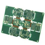
<img src="https://www.gopcba.com/wp-content/uploads/2026/08/high_density_pcb.jpg" alt="LoRa module mounted near the board edge with antenna keep-out” />
Dividing A Small Board Into Quiet And Noisy Regions
Before any routing begins, split the board into a digital region, an analogue region and a radio region, and write that split into the placement rules. The switch mode supply, the crystal, the high speed clocks and the memory bus belong at one end. The radio module and its antenna network belong at the other, ideally on the opposite edge of the board from the switching node.
What matters is the return path, not the visual separation. A sensitive receiver that sits above a grumbled ground plane shared with a switching regulator will pick up the switching harmonics on its own reference. Splitting the plane into an analogue section and a digital section joined at a single point, and then routing the module so that no digital trace crosses the analogue region, is what turns the floor plan into isolation.
Wiring The Serial Link To The Host
Almost all small radio modules present an SPI interface, with clock, master out, master in and chip select. The clock on such a link can run in the low tens of megahertz, which is fast enough to matter. Keep the four lines short, keep them together as a group, and reference them to a continuous ground plane on the adjacent layer so that the return current follows the signal.
Series termination at the driver is usually enough to control overshoot, but on a long link the clock is what limits the usable rate. Treat chip select as a signal rather than as a control line, because a slow dirty edge on chip select produces more spurious emissions than a clean clock. Where the module sits on a daughter card, use castellated holes at the module edge so that the interconnect stays short and the ground pins remain adjacent to the signal pins.
Antenna Placement And The Keep-Out
The antenna is where most compact designs lose their range. A chip antenna or a printed inverted F antenna needs a clear volume around it, free of copper, batteries, shields and the enclosure’s own metal, and that volume is defined by the antenna vendor rather than chosen by the designer. Ignoring the antenna keep-out to gain a few square millimetres of routing space will cost several decibels.
Under the antenna region, ground must be removed on every layer. This is one of the few places in a design where an apparently solid plane is harmful, because the plane detunes the element and shorts part of the radiating current. The feed line from the module to the antenna should be a controlled impedance trace, kept as short as possible, with the ground reference continuous on the layer below.
Supply Decoupling And Ground Stitching
A transmitter drawing a few hundred milliamperes in bursts will expose any weakness in the supply path. Bulk capacitance close to the module absorbs the slow part of the demand, and a small ceramic capacitor at the supply pin handles the fast edge. Placing every capacitor on a stub of its own defeats the purpose: the loop from pin through capacitor back to ground must be short and wide.
The ground structure deserves the same care. Stitch the ground planes with vias on a regular grid, and add extra stitching along the boundary between the radio region and the digital region so that return currents are not forced to detour. Where the design uses a stackup chosen to reduce emissions, keeping signal layers adjacent to solid planes is what makes the stackup effective rather than decorative.

Shared Supply Rails And Filtering
Many IoT products power the radio and the microcontroller from the same rail, which is convenient and risky. The radio’s own low dropout regulator and the module’s internal filtering help, but the host side still benefits from a ferrite bead or a small inductor in series with the digital supply branch, together with local bulk capacitance. The goal is to keep digital noise out of the radio supply and radio bursts out of the sensor supply.
Where the same rail feeds an analogue front end, order matters. Feed the analogue section through its own filter, and place the regulator, not the load, closest to the battery connector. Reusing a single regulator for a sensor amplifier and a transmitter that switches hundreds of milliamperes is one of the most reliable ways to introduce noise that no amount of capacitance will remove.
Pre-Compliance Testing And Field Behaviour
Regulatory testing is done on the finished product, so the value of pre-compliance measurements is early warning. Radiated emissions from the digital section, the effective radiated power of the antenna, and the receiver sensitivity in the presence of the host’s own clocks can all be measured on a development board with modest equipment, and all of them are influenced by the PCB rather than by the radio.
Consider also how the product will be tested in service, because range figures quoted in open air rarely survive an installation inside a metal cabinet. If the enclosure is conductive, the antenna must be brought to the outside face through a defined opening, and the feed and ground structure must be planned alongside that decision. Deciding this late forces a redesign of the mechanical part and the board together.
Additional Considerations for This Build
Practical attention to RF layout pays for itself here, because it is one of the items that decides whether the finished board behaves as the drawing intended. Where the requirement is not stated on the fabrication drawing or in the assembly notes, the shop has to assume a default, and that default is rarely the value the design was simulated with. Stating RF layout explicitly, together with the tolerance that applies, removes the assumption and keeps the result predictable from batch to batch.
Related reading: our fabrication notes, board quality and design release notes cover the same ground.
FAQ
Can the antenna keep-out be reduced on a small board? Only with the antenna vendor’s agreement and a measured result. Shrinking the keep-out detunes the element, shifts the resonant frequency and reduces efficiency, and the loss usually cannot be recovered by increasing transmit power without exceeding the regulatory limit.
Is a separate ground plane for the radio worth the effort? Usually yes on a mixed board, provided the two grounds are joined at one controlled point. Two planes joined everywhere behave as one plane; two planes joined nowhere create a dipole that radiates the digital noise the split was meant to contain.
How much bulk capacitance does a transmit burst need? Size it from the burst current and the length of the burst, then verify with a scope probe at the module supply pin. A common starting point is several tens of microfarads, but the measured voltage dip during a transmit slot, not the nominal value, is what proves the design.