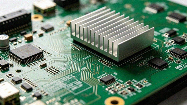
Laser Marking Serial Numbers on PCB Assemblies: Practical Notes
A serial number marked on the board is what allows a field failure to be traced back to a manufacturing lot, and laser marking has become the usual way of applying it because nothing touches the surface and nothing is consumed. The mark has to survive the assembly process, the conformal coating and the environment, and it has to be readable by the equipment that will use it.
Why Mark on the Board
A label can fall off, be covered by a coating or be removed during rework, while a mark made in the surface of the material cannot be separated from the product. That permanence is the reason board level traceability is normally built around a marked identifier rather than a label.
The identifier is also machine readable, which links the physical board to the process records. A data matrix code scanned at each station records which machine, which programme and which operator handled the assembly, and the same code can retrieve those records years later.
Marking Methods Compared
Inkjet printing is fast and cheap, but the ink sits on the surface and can be removed by cleaning solvents or rubbed away by handling. It is adequate for a mark that only has to survive the assembly line and is a poor choice for a product that will be exposed to the environment.
Laser marking changes the material itself, either by removing a thin layer of coating to expose the material underneath or by causing a local change in colour. The result is permanent, resistant to most solvents and compatible with the automated readers used on the line.
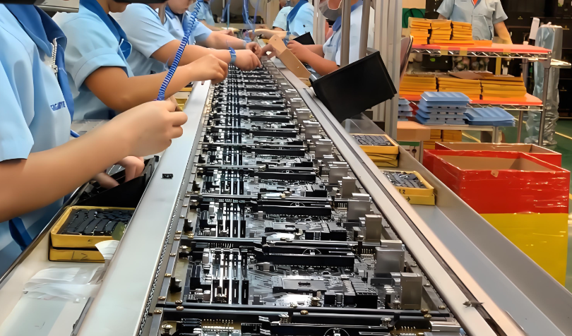
Laser Parameters and Material Interaction
The interaction depends on the material and on the wavelength of the laser. Solder mask responds well to a mark that removes a thin layer of the coating, while bare laminate, metal and ceramic each behave differently and may need different settings.
Power, frequency, marking speed and focus all affect the result, and a setting that produces a clean mark on one panel can produce a brown, smeared mark on the next if the coating thickness varies. The settings should be developed for a specific material and then verified on each batch. Our fabrication notes checklist lists the records worth keeping.
Data Matrix Codes and Readability
A data matrix is the usual format because it holds a useful amount of data in a small area and includes error correction, so a partly damaged code can still be read. The module size, the quiet zone around the code and the contrast between the mark and the background all determine whether a reader can decode it.
The code has to be large enough for the reader that will scan it. A scanner with a wide field of view cannot resolve a very small module size at the same working distance, so the code size and the reader specification belong together in the design. Our AOI notes describe how the reading equipment is integrated.

Contrast, Legibility and Surface Finish
Contrast comes from the difference between the marked and unmarked surface, and it varies with the solder mask colour. A white or light mask gives less contrast against a laser mark than a dark green or black mask, and a mark on bare copper depends on how the finish oxidises.
Where contrast is marginal, the mark can be made deeper or the surface can be chosen for readability rather than appearance. That choice is usually made at the design stage, along with the position of the mark, and it is expensive to change afterwards.
Marking Position and Assembly Clearance
The mark has to be somewhere the reader can reach it after assembly, which means it should not be covered by a component, a shield can or a connector body. Placing it on the top side in an area that stays clear after reflow is the simplest arrangement.
Clearance around the mark is needed for the reader illumination and for the operator to see the code. Where the design is dense, marking on the bottom side or on a panel rail is an alternative, at the cost of complicating the reading step.
Verification and Read Rate Control
The verification of a marking process is a read rate rather than an appearance check. A grading standard defines the quality of the code, and the practical measure is the proportion of codes that a defined reader can decode on the first attempt.
First pass read rate should be monitored, because a mark that is marginal produces a line that stops repeatedly. A reader that fails on a small percentage of boards costs far more in production time than the marking process itself.
Durability and Environmental Testing
The mark has to survive the process and the product life, so it is tested in the same way as the coating and the finish. Solvent resistance, abrasion, humidity and thermal cycling are the usual checks, and the test conditions should represent the actual environment rather than a generic laboratory exposure.
The result is a decision about the marking method rather than the laser settings alone. Where a mark has to survive abrasion, the method that removes material rather than one that changes colour is normally the better choice. Our judging PCB quality notes describe how the evidence is recorded.
Specifying Marking Requirements
The specification should state the marking method, the code format, the content of the code, the position and the required read rate. It should also state the durability test that the mark has to pass, because a permanent mark and a durable mark are not necessarily the same thing.
Where the marking is used for traceability, the data that the code points to has to be defined and retained. Our design release checklist includes the traceability items that have to be settled before production begins.
Process Control and Verification
On a design of this kind, laser marking is the item that decides how the rest of the board is arranged. A stack-up that is drawn rather than described removes most of the ambiguity from a quotation, and it lets the fabricator price the board against the dielectric and copper weights that will actually be used. Where the requirement is not written down, the shop supplies its own default, and the default is chosen for the process rather than for the design.
Process Control and Verification
On a design of this kind, laser marking is the item that decides how the rest of the board is arranged. A stack-up that is drawn rather than described removes most of the ambiguity from a quotation, and it lets the fabricator price the board against the dielectric and copper weights that will actually be used. Where the requirement is not written down, the shop supplies its own default, and the default is chosen for the process rather than for the design.
FAQ
Does laser marking damage the board? A correctly developed process removes only a controlled amount of material. Excessive power can damage the laminate or the mask, so the settings are verified on a sample before production and monitored afterwards.
Can a mark be added after conformal coating? It can, but the coating has to be penetrated and the result may be poorer. Marking before coating is the usual order, provided the coating is transparent enough for the code to be read through.
How does gopcb handle board marking? We agree the code content and position with the customer, develop the laser parameters for the specific mask and surface, verify the read rate with the customer reader where possible, and record the marking programme against the lot.