DC-DC Layout and Routing Points for Switching Converters
A switching converter is a small circuit with large currents, and the board around it is part of the circuit. The loop that carries the switching current has inductance that the schematic does not show, and every millimetre of it contributes to ringing at the switch node, to radiated noise and to the losses that show up as heat. DC-DC layout is therefore about geometry, not about component values.
Most of the work is done before routing begins. Placing the input capacitor, the switch and the return path so that the high current loop encloses the smallest possible area is the single decision that determines whether the converter behaves. Feedback routing and thermal design then decide how repeatable the result is in production.
The Hot Loop Comes First
The hot loop is the path the current takes during the on time of the switch: from the input capacitor, through the switch, through the inductor, and back to the capacitor through the ground. It carries a square wave with fast edges, and its area determines both the inductance that causes ringing and the field that radiates.
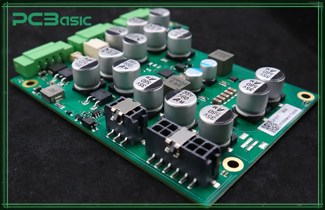
Placing the input capacitor directly across the switch and its return keeps that area small. The capacitor that does the work is the small ceramic part next to the device, not the bulk electrolytic at the edge of the board, and treating the two as interchangeable is one of the most common DC-DC layout mistakes.
Input Capacitor Placement and Its Return
Even a well placed input capacitor is defeated by a long return. If the current has to travel around the device to reach the capacitor ground, the loop area is set by that detour rather than by the distance to the capacitor. The return should run under or beside the forward path, on a plane if one is available.
Two capacitors of different values are usually placed in parallel, and the smaller one should be closest to the pins. The larger part can sit further away, because its job is to supply charge over a longer interval rather than to absorb the edge. Both need a low impedance connection to the same ground reference.
Switch Node and Inductor Routing
The switch node is the noisiest copper on the board. It swings at the input voltage with edges of a few nanoseconds, and its capacitance to everything nearby couples that noise into whatever it touches. The copper should be no larger than it needs to be, and nothing sensitive should be routed beneath or beside it.
The inductor belongs close to the switch, and its connection should be short and wide. A long trace between the switch and the inductor adds inductance in the loop that carries the full load current, which increases both the switching loss and the radiated field. This is a case where a few millimetres genuinely matter.
Feedback and Sense Routing
Feedback routing determines the accuracy of the output, because the divider measures the voltage at the point where it is connected. Sensing at the far end of a trace that carries the load current means the regulation includes the drop along that trace, and the error changes with load.
The divider should be connected to the output at the point where regulation is wanted, with a short and quiet connection. The feedback node is high impedance and therefore sensitive, so it should be kept away from the switch node and from the inductor, and its trace should not run parallel to any switching signal.
Thermal Vias and Copper Area
Thermal vias under the exposed pad of the controller and under the switch carry heat into the copper on the other layers. Their number and diameter are set by the thermal resistance required, and they should be connected to a copper area large enough to spread the heat rather than to a small island.
The copper that carries the load current also radiates heat, so the layout and the thermal design are the same exercise. Widening a trace to reduce its temperature rise also reduces its resistance, which improves the efficiency of the converter and reduces the temperature of everything around it.
Verification Before Release
Once the board is routed, the loops can be checked on the screen. Measuring the area enclosed by the high current path on each layer, confirming that the return is continuous, and looking at the switch node copper as a radiator are quick reviews that catch most of the geometry mistakes.
The remaining risk is in the parts of the design that will be built by someone else. The requirements that matter to the fabricator, including copper weight and via treatment, belong in the fabrication notes, while the assembly related choices follow the same reasoning as any other DC-DC converter layout review that has to survive a volume build.
Process Control and Verification
On a design of this kind, hot loop is the item that decides how the rest of the board is arranged. Keeping a sample from the panel turns a dispute into a measurement, because the same coupon can be re-examined by both parties without rebuilding the batch. Reviewing the design before the data is released is cheaper than correcting it after the panel is in the tank, because every step downstream inherits the decision made at the front end.
Documenting the assumption is part of the design work, and a short note on the drawing prevents a question that would otherwise arrive a day later and cost a day of schedule. The process window is set by the narrowest step in the flow, so an improvement anywhere else shows up as margin rather than as yield until that step is addressed.
A short note on the drawing about handling, storage or packaging is often worth more than an extra decimal place on a tolerance.
Related reading: our fabrication notes, board quality and design release notes cover the same ground.
Process Control and Verification
On a design of this kind, hot loop is the item that decides how the rest of the board is arranged. Keeping a sample from the panel turns a dispute into a measurement, because the same coupon can be re-examined by both parties without rebuilding the batch. Reviewing the design before the data is released is cheaper than correcting it after the panel is in the tank, because every step downstream inherits the decision made at the front end.
Process Control and Verification
On a design of this kind, hot loop is the item that decides how the rest of the board is arranged. Keeping a sample from the panel turns a dispute into a measurement, because the same coupon can be re-examined by both parties without rebuilding the batch. Reviewing the design before the data is released is cheaper than correcting it after the panel is in the tank, because every step downstream inherits the decision made at the front end.
FAQ
Can a converter be laid out on two layers? Yes, provided a continuous ground plane is available on the second layer and the high current loop stays compact. Once the loop has to route around the board, more layers are the cheaper answer.
Does the switch node really need to be small? Yes. Its copper is a capacitor to everything around it and an antenna for the switching edge, and neither effect helps the converter.
How is a converter layout verified? By measuring the switching waveform and the radiated field on a first article, and by checking the loop areas on the layout before release. The bench measurement confirms what the geometry predicted.