



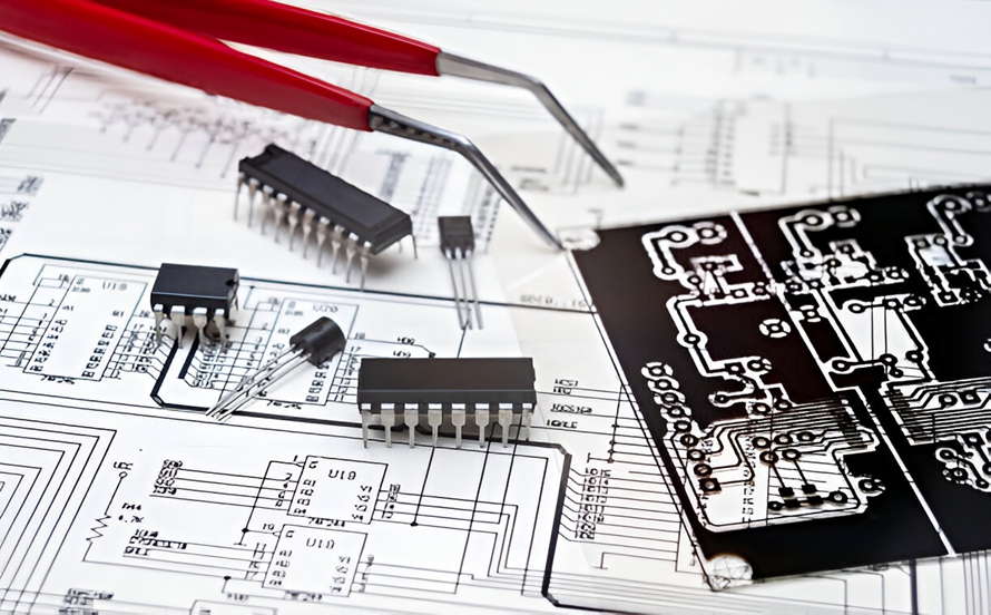
What Is PCB Prototyping? PCB Design, PCB Manufacturing & Prototype Development Guide
Modern PCB Design and manufacturing technologies have made enormous advances in functionality, miniaturization, durability, processing speed, and reliability. From smartphones and laptops to automotive electronics, industrial controllers, medical equipment, and communication systems, virtually every modern electronic product depends on printed circuit boards (PCBs).
However, a successful electronic product is not created simply by designing a circuit and sending the files directly to mass production. A reliable PCB typically goes through a systematic process that includes requirements planning, schematic development, PCB layout, prototype fabrication, assembly, testing, validation, and design iteration.
One of the most common mistakes in PCB Manufacturing is moving into mass production before the design and its manufacturing robustness have been adequately verified. A design may appear correct in simulation or on a computer screen but still encounter manufacturing, assembly, electrical, thermal, or mechanical problems when converted into a physical product.
This is where PCB prototyping becomes essential.
PCB prototyping provides a practical way to transform a design concept into a physical circuit board, evaluate its performance, identify potential problems, and optimize the design before committing to large-scale production.
So, what is PCB prototyping, and why is it important? This guide explains the definition, process, benefits, testing requirements, and best practices of PCB prototyping.
What Is PCB Prototyping?
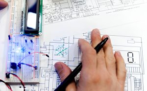
PCB prototyping is the process of creating one or more physical prototype circuit boards to verify a PCB design before full-scale production.
A PCB prototype typically goes through some or all of the following stages:
- Requirements definition
- Schematic design
- Bill of materials (BOM) development
- PCB layout
- Design Rule Check (DRC)
- Gerber and manufacturing-file generation
- Prototype PCB fabrication
- PCB assembly
- Electrical and functional testing
- Design evaluation
- Design iteration
The primary objective is to identify design and manufacturing problems as early as possible.
For example, a prototype can reveal problems such as:
- Incorrect component footprints
- PCB routing conflicts
- Insufficient copper clearance
- Incorrect hole sizes
- Poor component placement
- Signal integrity problems
- Thermal management issues
- Soldering defects
- Component availability problems
- Manufacturing tolerances that were overlooked
- Mechanical interference
- Electrical performance deviations
Instead of discovering these problems after thousands of boards have been manufactured, engineers can identify and correct them during the prototype stage.
Therefore, PCB prototyping is not simply the production of a small number of circuit boards. It is a structured engineering validation process that connects PCB Design, PCB Manufacturing, assembly, and testing.
What Are the Steps in PCB Prototyping?
PCB prototyping involves close cooperation among designers, engineers, procurement teams, PCB manufacturers, and assembly specialists.
The exact workflow varies depending on board complexity, application requirements, production volume, and reliability requirements. However, a typical prototype development process includes the following steps.
1. Define Project Requirements
Requirements planning is the starting point of PCB prototyping.
Before creating a schematic or PCB layout, engineers should define the functional, electrical, mechanical, thermal, environmental, and regulatory requirements of the product.
Important considerations may include:
- Operating voltage and current
- Signal frequency
- Number and type of interfaces
- PCB dimensions
- Number of layers
- Required impedance
- Operating temperature
- Mechanical constraints
- Component availability
- Expected production volume
- Reliability requirements
- Applicable industry standards
Clearly defined requirements provide a foundation for subsequent PCB Design and manufacturing decisions.
A prototype is only useful if it is evaluated against clearly defined performance targets.
2. Create the PCB Schematic
The schematic converts the functional concept into an electrical representation.
Engineers use electronic design automation (EDA) tools to place components and establish electrical connections between them. Popular PCB design platforms include Altium Designer, Cadence tools, KiCad, and other professional EDA systems.
At this stage, engineers should verify:
- Component values
- Net connections
- Power distribution
- Grounding
- Protection circuits
- Interface connections
- Component ratings
- Critical signal paths
The schematic is the electrical foundation of the PCB and directly influences the subsequent layout.
3. Create the Bill of Materials (BOM)
A complete Bill of Materials (BOM) identifies the components required to build the prototype.
A typical BOM may include:
- Manufacturer part number
- Component description
- Quantity
- Package type
- Supplier
- Approved alternatives
- Lifecycle status
- Electrical specifications
Component availability is particularly important during prototyping.
A theoretically perfect design can still experience delays if critical components are obsolete, unavailable, or subject to long lead times. Therefore, engineers should identify alternative components where appropriate and verify that replacement parts are electrically and mechanically compatible.
4. Develop the PCB Layout
Once the schematic has been verified, engineers convert the electrical design into a physical PCB layout.
PCB layout determines the physical location of components, copper traces, vias, planes, mounting holes, and other board features.
During layout development, engineers should consider:
- Component placement
- Routing strategy
- Power and ground planes
- Signal integrity
- Thermal management
- Electromagnetic compatibility (EMC)
- Electromagnetic interference (EMI)
- Creepage and clearance
- Manufacturing tolerances
- Assembly accessibility
- Board dimensions
For high-speed or high-frequency designs, additional considerations such as controlled impedance, return paths, stack-up design, and transmission-line geometry may become critical.
Good layout design should achieve not only electrical functionality but also manufacturability and assembly reliability.
5. Perform Design Rule Check (DRC)
Design Rule Check (DRC) is an important validation step before manufacturing.
DRC verifies whether the PCB layout complies with predefined design and manufacturing constraints.
Typical checks include:
- Minimum trace width
- Minimum clearance
- Via dimensions
- Hole sizes
- Pad dimensions
- Copper-to-edge clearance
- Solder mask clearance
- Component spacing
- Manufacturing constraints
However, passing DRC does not guarantee that the PCB will work correctly.
DRC primarily checks whether the design conforms to defined rules. Engineers must still conduct electrical, functional, thermal, mechanical, and manufacturability reviews.
6. Generate Gerber and Manufacturing Files
After the PCB layout has been completed and reviewed, manufacturing data must be generated.
Common PCB manufacturing documentation may include:
- Gerber files
- NC drill files
- Stack-up information
- Fabrication drawings
- Solder mask information
- Surface-finish requirements
- Controlled-impedance requirements
- PCB specifications
- Assembly drawings
- Pick-and-place files
- BOM
Gerber remains one of the most widely used formats for communicating PCB fabrication information.
The manufacturing package should be carefully checked before being released to the PCB manufacturer.
7. Prototype PCB Manufacturing
The approved manufacturing files are sent to a PCB fabrication facility to produce the prototype boards.
A typical PCB Manufacturing process may include:
Inner-Layer Processing
For multilayer PCBs, inner copper layers are imaged, developed, etched, and inspected before lamination.
Lamination
Multiple layers of copper foil, core materials, and prepreg are stacked according to the specified stack-up and laminated under controlled heat and pressure.
Drilling
Through-holes, vias, and other required holes are drilled according to the manufacturing data.
Depending on the design, mechanical drilling or laser drilling may be used.
Copper Plating
For multilayer and plated-through-hole boards, conductive copper is deposited onto hole walls and relevant surfaces to establish electrical connections between layers.
Outer-Layer Processing
The outer copper circuitry is formed and processed according to the required PCB pattern.
Etching
Unwanted copper is removed to create the required conductive pattern.
Solder Mask Application
Solder mask is applied to protect exposed copper and reduce the risk of unintended solder bridging during assembly. Openings are created where soldering or electrical contact is required.
Surface Finish
A suitable surface finish is applied to exposed copper pads to improve solderability and protect the copper surface.
Common options include HASL, lead-free HASL, ENIG, OSP, immersion tin, immersion silver, and ENEPIG.
Silkscreen
Reference designators, polarity marks, labels, logos, and other identification information may be printed on the board.
Bare-Board Testing
Before assembly, the prototype PCB can undergo electrical testing to identify problems such as unintended opens or shorts.
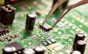
Testing the bare board before component installation can prevent defective PCBs from moving into the more expensive assembly stage.
8. PCB Assembly
After the bare PCB passes the required inspections and tests, components are installed.
PCB assembly may involve Surface Mount Technology (SMT), Through-Hole Technology (THT), or a combination of both.
Solder Paste Printing
For SMT assembly, solder paste is deposited onto designated pads using a stencil.
The quality of solder paste printing has a major influence on solder-joint reliability.
Important factors include:
- Stencil thickness
- Aperture design
- Paste volume
- Printing pressure
- Printing speed
- PCB support
- Paste condition
Component Placement
Automated pick-and-place equipment positions components according to the placement data.
Component orientation, polarity, package type, and placement accuracy must be carefully controlled.
Reflow Soldering
After component placement, the assembled board passes through a reflow oven.
The board follows a controlled thermal profile designed for the specific solder paste, components, PCB construction, and assembly requirements.
The objective is to create reliable solder joints without exposing components or the PCB to inappropriate thermal conditions.
Visual Inspection and Automated Inspection
After soldering, the prototype can be inspected using:
- Visual inspection
- Automated Optical Inspection (AOI)
- X-ray inspection where appropriate
AOI can identify many surface-level defects, while X-ray inspection can be useful for inspecting hidden solder joints such as bottom-terminated components and certain BGA packages.
Typical defects may include:
- Solder bridges
- Insufficient solder
- Component misalignment
- Missing components
- Tombstoning
- Poor solder joints
- Voids
- Incorrect component orientation
9. PCBA Testing and Functional Verification
Assembly inspection alone does not prove that a prototype is electrically functional.
The assembled PCBA should therefore undergo appropriate electrical and functional testing.
Depending on the product, testing may include:
- Power-on testing
- Voltage and current measurements
- Continuity testing
- ICT
- Functional testing
- Communication-interface testing
- Clock and timing verification
- Sensor testing
- Firmware/software interaction
- Thermal testing
- Signal-integrity verification
For example, a communication board may need to verify interfaces such as USB, Ethernet, CAN, UART, SPI, or I²C.
A power-management board may require detailed verification of output voltage, current capability, protection functions, thermal behavior, and transient response.
The testing strategy should be developed according to the actual product requirements rather than relying on a single universal test method.
10. Analyze Results and Iterate the Design
One of the most important characteristics of PCB prototyping is iteration.
If testing identifies a problem, engineers should determine its root cause before making modifications.
Possible corrective actions may include:
- Changing component values
- Replacing components
- Modifying PCB traces
- Adjusting component placement
- Changing the PCB stack-up
- Increasing copper width
- Improving thermal paths
- Revising grounding
- Changing the enclosure interface
- Selecting a different PCB material
- Improving assembly parameters
After the design is modified, a new prototype may be manufactured and tested.
This cycle can be repeated until the design meets the required functional, electrical, mechanical, thermal, reliability, and manufacturing targets.
This is the real value of PCB prototyping: it transforms a theoretical design into a validated and manufacturable product.
What Are the Benefits of PCB Prototyping?
Although PCB prototyping requires additional time and resources, it can significantly reduce engineering and manufacturing risks.
1. Higher Production Yield
One of the primary goals of prototyping is to create a design that is not only functional but also manufacturable.
A prototype allows engineers to identify problems before mass production.
For example, a design may function electrically but still have:
- Difficult-to-manufacture features
- Insufficient component clearance
- Poor solderability
- Inadequate thermal management
- Difficult assembly access
- Excessively tight tolerances
Correcting these problems during prototyping can improve production yield when the product enters volume manufacturing.
2. Improved Product Quality
PCB prototyping provides an opportunity to compare actual product performance against design requirements.
During prototype evaluation, engineers can identify deviations in:
- Electrical performance
- Mechanical dimensions
- Thermal behavior
- Assembly quality
- Signal integrity
- Component compatibility
- Reliability
The resulting data can then be used to improve the design and manufacturing process.
3. Faster Time to Market
At first glance, prototyping appears to add time to product development.
However, skipping prototyping can create much greater delays later.
Discovering a serious design problem after mass production may require:
- Production stoppages
- PCB redesign
- Component replacement
- Rework
- Scrap
- Additional testing
- Product recalls
Early prototype validation helps prevent these problems and can ultimately shorten the overall development cycle.
4. Lower Development and Manufacturing Costs
PCB prototyping can significantly reduce the financial risk associated with large-scale production.
Producing a small number of prototypes is generally much less expensive than discovering a fundamental design problem after manufacturing thousands of units.
Prototype validation can help reduce:
- Scrap costs
- Rework costs
- Engineering changes
- Production downtime
- Component waste
- Warranty claims
- Recall risks
Therefore, prototyping should be viewed as an investment in risk reduction rather than simply an additional manufacturing expense.
5. Better DFM and DFA
A prototype can reveal whether a design is truly suitable for manufacturing and assembly.
Design for Manufacturing (DFM) focuses on whether the PCB can be fabricated efficiently and consistently.
Design for Assembly (DFA) focuses on whether components can be placed and soldered reliably.
A prototype provides valuable feedback about both.
This is especially important for complex boards with:
- Fine-pitch components
- BGA packages
- HDI structures
- High layer counts
- Controlled impedance
- High component density
- Mixed SMT/THT assembly
PCB Prototyping vs. Mass Production
PCB prototyping and mass production have different objectives.
| Feature | PCB Prototyping | Mass Production |
|---|---|---|
| Primary objective | Design validation | Volume manufacturing |
| Quantity | Small | Medium to large |
| Design flexibility | High | Lower after release |
| Engineering changes | Expected | Minimized |
| Testing focus | Design verification | Process and quality control |
| Cost per board | Usually higher | Usually lower |
| Main risk | Design uncertainty | Process variation and yield |
A prototype should therefore not be judged only by its unit cost.
The more important question is whether the prototype provides enough information to confidently release the product into volume PCB Manufacturing.
How to Choose a PCB Prototyping Partner
Selecting the right manufacturing partner can significantly influence prototype quality and development speed.
Engineers and purchasing teams should evaluate a supplier based on:
PCB Fabrication Capability
Check whether the manufacturer supports the required:
- Layer count
- Board thickness
- Copper thickness
- Material
- Minimum trace/space
- Via structures
- Surface finish
- Impedance requirements
- HDI technology
- Rigid-flex construction
PCB Assembly Capability
The supplier should also have appropriate SMT and THT assembly capabilities, especially when the prototype uses fine-pitch or high-density components.
Testing Capability
A capable supplier should provide suitable inspection and testing options such as AOI, X-ray, ICT, functional testing, and electrical testing according to the project requirements.
Engineering Support
Prototype development often requires engineering communication rather than simply manufacturing according to uploaded files.
A strong supplier should be able to support:
- DFM review
- BOM verification
- Component alternatives
- Stack-up recommendations
- Manufacturing feedback
- Assembly optimization
- Prototype troubleshooting
For companies looking for an integrated development and manufacturing partner, Kingda provides PCB design, PCB fabrication, PCB assembly, testing, and related PCBA manufacturing services. This type of one-stop workflow can simplify communication between design, fabrication, assembly, and testing teams.
Common PCB Prototyping Mistakes
Several mistakes can reduce the value of a PCB prototype.
Skipping DFM Review
Passing DRC does not necessarily mean a PCB is optimized for manufacturing.
A design should also be reviewed against the actual manufacturer’s fabrication and assembly capabilities.
Using Unavailable Components
A prototype can be delayed if the BOM contains obsolete, allocated, or long-lead-time components.
Component availability should therefore be considered during the design stage.
Testing Only the Bare PCB
A bare board can pass electrical testing and still fail after assembly.
Complete prototype validation should include both PCB fabrication and PCBA performance where applicable.
Focusing Only on Electrical Function
A prototype should also be evaluated for:
- Thermal performance
- Mechanical fit
- Assembly reliability
- EMC/EMI behavior
- Manufacturability
- Serviceability
Moving to Mass Production Too Early
A successful prototype does not necessarily mean that every production risk has been eliminated.
Before mass production, teams should confirm that the final design, BOM, manufacturing process, assembly process, test procedures, and quality requirements are all adequately controlled.
Final Thoughts
So, what is PCB prototyping?
PCB prototyping is the structured process of turning a PCB concept into a physical, assembled, tested, and validated product before committing to mass production.
It connects PCB Design with PCB Manufacturing by providing an essential validation stage between engineering development and volume production.
A well-executed prototype can identify design errors, manufacturing limitations, component problems, assembly defects, electrical issues, thermal problems, and mechanical interference before they become expensive production failures.
The goal of prototyping is therefore not simply to build a sample PCB. It is to build confidence in the final product.
For complex electronic products, working with an experienced partner capable of supporting PCB design, fabrication, assembly, testing, and engineering review can make the transition from prototype to mass production significantly smoother.
Article Summary
PCB prototyping is an essential part of modern electronic product development. It enables engineers to validate a design, identify manufacturing and assembly problems, test actual performance, and optimize the product before mass production. A complete process typically includes requirements planning, schematic development, BOM preparation, PCB layout, DRC, manufacturing-file generation, prototype fabrication, PCB assembly, testing, and design iteration.
By integrating PCB Design, DFM, PCB fabrication, assembly, and functional testing, PCB prototyping can improve product quality, increase production yield, reduce manufacturing risks, control development costs, and accelerate time to market.


