Single-Sided PCB: PCB Design, PCB Manufacturing, Advantages & Applications
Printed circuit board technology continues to evolve to meet increasingly complex requirements related to circuit layout, operating temperature, electrical performance, reliability, and cost. As a result, PCBs can be classified according to various factors, including substrate material, number of conductive layers, construction, and assembly technology.
A Single-Sided PCB is one of the simplest and most widely used PCB configurations. Unlike double-sided and multilayer boards, it has only one primary conductive copper layer for routing electrical connections. Its relatively simple construction makes it suitable for low-density circuits, cost-sensitive products, and applications where advanced routing capabilities are not required.
This article provides a comprehensive overview of single-sided PCBs, including their structure, materials, manufacturing process, design considerations, advantages, limitations, applications, quality standards, and comparison with double-sided PCBs.
What Is a Single-Sided PCB?
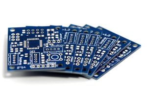
A Single-Sided PCB, also called a single-layer PCB or single-sided printed circuit board, is a circuit board with one primary conductive copper layer laminated onto one side of an insulating substrate.
The copper layer is patterned to form:
- Conductive traces
- Component pads
- Copper areas
- Ground or power connections where applicable
- Other required conductive features
Because there is only one primary routing layer, circuit traces cannot normally cross each other directly. Designers must therefore carefully plan the routing path and component placement.
Single-sided PCBs are particularly suitable for circuits with relatively low component density and straightforward electrical connections. Typical examples include LED boards, basic power supplies, calculators, simple control circuits, and certain consumer appliances.
Depending on the application, a single-sided PCB can be manufactured using rigid, flexible, or other specialized substrate systems. Components may be installed using Surface Mount Technology (SMT), through-hole technology (THT), or a combination of both.
Compared with complex multilayer boards, single-sided PCBs generally offer simpler manufacturing, lower material consumption, and lower production costs.
Types of Single-Sided PCBs
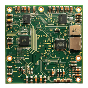
Single-sided PCBs can be categorized according to the substrate material and board construction used during manufacturing.
Common types include:
- FR-4 Single-Sided PCB
- FR-2 Single-Sided PCB
- Phenolic Paper Single-Sided PCB
- Flexible Single-Sided PCB
- Metal-Core Single-Sided PCB
Each construction has different electrical, mechanical, thermal, and cost characteristics.
FR-4 Single-Sided PCB
FR-4 is one of the most widely used materials for rigid PCBs. It consists primarily of woven glass fabric reinforced with epoxy resin.
FR-4 offers a useful balance of:
- Mechanical strength
- Electrical insulation
- Thermal stability
- Manufacturability
- Cost
Different FR-4 grades have different Tg, dielectric properties, thermal expansion characteristics, and other performance parameters. Therefore, the appropriate FR-4 grade should be selected according to the application rather than treating all FR-4 materials as identical.
FR-2 Single-Sided PCB
FR-2 is a paper-based phenolic laminate that is generally used for relatively simple and cost-sensitive electronic products.
Compared with FR-4, FR-2 typically offers lower thermal and mechanical performance but can provide an economical solution for applications with modest operating requirements.
CEM-1 Single-Sided PCB
CEM-1 is a composite epoxy material commonly based on a paper core with glass-fiber reinforcement in selected construction layers.
It can provide a cost-effective alternative for certain simple rigid PCB applications where the performance requirements do not justify more advanced laminate materials.
Flexible Single-Sided PCB
A flexible single-sided PCB uses a flexible substrate, commonly polyimide, instead of a conventional rigid laminate.
It can bend or conform to a curved structure and is therefore useful in:
- Wearable electronics
- Medical devices
- Cameras
- Display systems
- Compact consumer electronics
- Automotive interconnects
Metal-Core Single-Sided PCB
A metal-core PCB incorporates a metal substrate, commonly aluminum, to improve heat dissipation.
Metal-core single-sided boards are particularly useful for applications with significant thermal loads, such as:
- LED lighting
- Power electronics
- Motor control
- Automotive lighting
- High-power converters
The exact thermal performance depends on the metal substrate, dielectric layer, copper thickness, thermal interface design, and overall system construction.
Structure of a Single-Sided PCB
The basic construction of a single-sided PCB is relatively simple. It generally consists of a substrate, one copper layer, solder mask, and silkscreen.
1. Substrate or Insulating Base Material
The substrate provides the mechanical foundation of the PCB and electrically isolates the copper conductor from the surrounding environment.
Common substrate materials include:
- FR-4
- FR-2
- CEM-1
- Polyimide
- Aluminum-based metal-core constructions
The substrate should be selected according to mechanical strength, operating temperature, dielectric requirements, flexibility, thermal management, and cost.
2. Copper Conductive Layer
The copper layer is the primary electrical pathway of a single-sided PCB.
After the PCB manufacturing process defines the circuit pattern, the copper layer forms the required traces and pads.
Copper thickness is an important design parameter because it affects:
- Current-carrying capability
- Trace resistance
- Heat generation
- Mechanical robustness
- Manufacturing cost
Higher-current applications may require thicker copper than conventional low-power boards.
3. Solder Mask
The solder mask is a protective polymer coating applied over selected copper areas. It helps prevent unintended solder bridges, protects exposed circuitry from contamination, and provides additional electrical insulation.
Green is the most common solder mask color, but other colors such as black, blue, red, white, and yellow can also be used.
Importantly, component pads and other areas that must be soldered remain exposed through openings in the solder mask.
4. Silkscreen
The silkscreen is used to print reference designators, polarity indicators, component labels, logos, warnings, and other manufacturing or assembly information.
Although the silkscreen does not normally contribute to the electrical function of the circuit, it improves assembly efficiency, inspection, troubleshooting, and maintenance.
Materials Used in Single-Sided PCB Manufacturing
Material selection is an important part of PCB Design because the substrate influences the board’s mechanical strength, thermal behavior, electrical properties, and manufacturing cost.
| Material | Main Characteristics | Typical Applications |
|---|---|---|
| FR-4 | Strong, reliable, widely available | General-purpose rigid PCBs |
| FR-2 | Economical paper-based laminate | Simple, cost-sensitive electronics |
| CEM-1 | Cost-effective composite laminate | General low-to-medium complexity applications |
| Polyimide | Flexible and thermally capable | Flexible and rigid-flex circuits |
| Aluminum metal core | High thermal conductivity relative to conventional rigid laminates | LED and power electronics |
FR-4
FR-4 is a broad family of flame-retardant glass-reinforced epoxy laminates.
It is widely used because it provides a good combination of:
- Mechanical strength
- Electrical insulation
- Dimensional stability
- Manufacturability
- Cost effectiveness
However, not every FR-4 grade has the same thermal or electrical characteristics. Designers should select a specific laminate based on the manufacturer’s datasheet and application requirements.
CEM-1
CEM-1 is frequently considered when cost is a major consideration and the application does not require the full performance range of higher-grade FR-4 materials.
Its suitability depends on the required mechanical, thermal, and electrical performance.
FR-2 and Phenolic Materials
FR-2 is commonly used for simple, low-cost products where high thermal performance is not a primary requirement.
It can be suitable for basic electronic circuits but is generally less capable than modern high-performance FR-4 materials.
Polyimide
Polyimide is widely used in flexible circuits because of its flexibility and thermal characteristics.
In a flexible single-sided PCB, the copper conductor may be bonded to a polyimide film and protected using coverlay or another suitable protective structure.
Metal-Core Materials
Metal-core PCBs use an electrically insulating dielectric layer between the conductive copper and metal base.
Aluminum is particularly common because it combines relatively low weight, good thermal conductivity, availability, and cost effectiveness.
Advantages of Single-Sided PCBs
Single-sided PCBs remain popular because their simple construction provides several practical benefits.
Simple PCB Design
With only one primary conductive layer, routing is easier to understand and manufacture.
The simpler layout can also make:
- Design verification easier
- Troubleshooting more straightforward
- Manufacturing more predictable
- Documentation simpler
However, the lack of a second routing layer also creates important routing limitations.
Lower Manufacturing Cost
A single-sided PCB generally requires fewer conductive and dielectric structures than a double-sided or multilayer board.
Lower material consumption and simpler processing can reduce manufacturing costs, especially in high-volume applications.
Shorter Production Cycle
Because the board structure is relatively simple, single-sided PCBs can often be manufactured more quickly than complex multilayer boards.
Actual lead time depends on board specifications, quantity, materials, surface finish, testing requirements, and production capacity.
Easy Inspection and Repair
The simple structure makes visual inspection and troubleshooting relatively straightforward.
Components and conductive traces can generally be accessed more easily than those embedded within a complex multilayer structure.
Suitable for High-Volume Cost-Sensitive Products
When an application does not require multilayer routing, a single-sided PCB can provide a practical balance between functionality and manufacturing cost.
This is particularly important for products produced in large quantities.
Lightweight Construction
A simple single-sided PCB can be relatively thin and lightweight, particularly when a thin laminate or flexible substrate is selected.
However, the actual board weight depends on the substrate thickness, copper weight, board dimensions, components, and mechanical requirements.
Limitations of Single-Sided PCBs
When multiple signals need to cross one another, designers cannot simply route one signal on another copper layer as they would on a double-sided or multilayer board.
Instead, designers may need to:
- Rearrange components
- Increase trace length
- Increase board dimensions
- Use jumpers
- Modify circuit topology
- Simplify the circuit
These approaches can increase design complexity or board size.
Lower Component Density
Because routing space is limited, single-sided boards generally cannot accommodate the same component density as advanced multilayer PCBs.
This makes them less suitable for:
- Complex processors
- High-density memory
- Advanced communication systems
- Large digital systems
- Highly integrated computing hardware
Limited Ground and Power Distribution
A single conductive layer makes it difficult to create large continuous power and ground planes.
This can affect:
- Voltage distribution
- Return-current paths
- Electromagnetic compatibility
- Noise performance
- Signal integrity
For simple low-speed circuits, these limitations may be manageable. For high-speed or sensitive designs, a multilayer structure may be more appropriate.
Thermal Management Challenges
Conventional FR-4 or paper-based single-sided PCBs have limited ability to spread heat compared with dedicated metal-core PCB structures.
Designers may need to use:
- Wider copper areas
- Thermal vias where applicable
- Heat sinks
- Improved component spacing
- External thermal interfaces
- Metal-core construction
Limited High-Speed Design Flexibility
A single-sided structure does not inherently prevent high-frequency operation. However, the absence of dedicated reference planes and additional routing layers can make controlled impedance, return-path management, and electromagnetic compatibility more difficult.
For demanding high-speed designs, engineers often select multilayer structures with carefully controlled stackups.
Single-Sided PCB Design Considerations
Although single-sided PCB design is relatively simple, several engineering factors should be considered.
1. Current-Carrying Capacity
Trace width and copper thickness must be selected according to the required current.
High-current traces should generally be wider and may require heavier copper. Designers should use appropriate IPC-based calculations and manufacturer design rules rather than relying on a single universal trace-width value.
2. Thermal Management
Heat-producing components should be positioned carefully.
Designers should consider:
- Component power dissipation
- Copper area
- Ambient temperature
- Airflow
- Heat sinks
- Thermal interfaces
- Distance between hot and temperature-sensitive components
For high-power applications, metal-core construction may be preferable.
3. Component Placement
Because all routing must be performed on one primary copper layer, component placement has a direct impact on routing feasibility.
A good layout should minimize unnecessary trace crossings and provide short, logical connections between related components.
4. Signal Integrity
For low-speed circuits, signal integrity may not be a major concern. However, faster signals can still experience:
- Crosstalk
- Electromagnetic interference
- Reflections
- Excessive trace length
- Poor return paths
Designers should evaluate these effects according to the actual signal speed and electrical requirements.
5. Board Size
Routing restrictions may force designers to increase board dimensions.
Therefore, the PCB designer should balance:
- Routing density
- Board dimensions
- Component placement
- Manufacturing cost
- Mechanical constraints
6. Hole and Slot Placement
Mounting holes, slots, cutouts, and component holes must be positioned carefully to avoid interfering with traces.
Adequate copper-to-hole and copper-to-edge clearances should be maintained according to the PCB manufacturer’s capabilities.
Single-Sided PCB Manufacturing Process
The PCB Manufacturing process for a single-sided PCB is generally simpler than that of a multilayer board, although the exact sequence varies according to the manufacturing method and product specifications.
Step 1: PCB Design
The process begins with schematic development and PCB layout.
The design defines:
- Circuit connectivity
- Component footprints
- Trace widths
- Pad sizes
- Board outline
- Mounting holes
- Copper areas
- Solder mask openings
- Silkscreen information
Gerber, drill, and other manufacturing files are then generated for fabrication.
Step 2: Copper-Clad Laminate Preparation
A suitable copper-clad laminate is selected according to the design requirements.
The panel surface is cleaned to remove contaminants that could affect photoresist adhesion or subsequent processing.
Step 3: Circuit Pattern Transfer
The desired circuit pattern is transferred onto the copper surface using an appropriate imaging process.
Modern PCB fabrication commonly uses photolithographic imaging rather than relying simply on conventional screen printing to define fine circuit patterns.
Step 4: Etching
The unwanted copper is chemically removed, leaving the required conductive traces and pads.
The remaining copper forms the electrical circuit.
Step 5: Drilling
Required component holes, mounting holes, and other mechanical holes are drilled.
The hole diameter and positional accuracy must correspond to the design documentation and component requirements.
Step 6: Deburring and Cleaning
After drilling, the board may undergo cleaning and deburring to remove residues and prepare the surface for subsequent processes.
Step 7: Solder Mask Application
Solder mask is applied and selectively exposed or developed so that solderable pads remain accessible while the rest of the circuitry is protected.
Step 8: Surface Finish
Exposed copper pads receive the specified surface finish to improve oxidation resistance and solderability.
Common options include:
- HASL
- Lead-free HASL
- ENIG
- Immersion silver
- Immersion tin
- OSP
The appropriate finish depends on the application, assembly process, storage requirements, and cost targets.
Step 9: Silkscreen Printing
Reference designators, polarity markings, logos, and other required information are printed on the PCB.
Step 10: Electrical Testing and Inspection
The finished board is inspected for manufacturing defects and tested for electrical continuity and isolation where required.
AOI may be used to identify visible defects, while electrical testing can detect open circuits and shorts.
Step 11: Routing, Profiling, and Final Inspection
The PCB panel is separated into individual boards through routing, punching, V-scoring, or another appropriate process.
Final inspection verifies dimensions, appearance, surface finish, and other customer-defined requirements.
After fabrication is complete, the bare PCB can proceed to SMT, THT, or other assembly processes.
IPC Standards for Single-Sided PCBs
Even though single-sided PCBs have a relatively simple construction, their quality should still be controlled according to appropriate industry standards.
Important standards may include:
IPC-A-600
IPC-A-600 defines visual and dimensional acceptability criteria for printed boards.
It covers characteristics such as:
- Conductor conditions
- Hole conditions
- Lamination characteristics
- Surface-related defects
- Dimensional characteristics
The exact acceptance criteria depend on the applicable class and product specification.
IPC-2221
IPC-2221 provides generic design guidance for printed board structures, including considerations related to conductor spacing, electrical requirements, mechanical design, and other design parameters.
Specific product designs may also require additional IPC standards.
IPC-4101
IPC-4101 addresses base materials used for rigid and multilayer printed boards.
Material selection should consider the appropriate specification, laminate construction, and electrical and thermal requirements.
IPC-TM-650
IPC-TM-650 provides standardized test methods used to evaluate various properties of printed boards and materials.
The exact test methods required depend on the board construction and customer requirements.
Importantly, IPC standards should not be treated as a single universal checklist. The applicable standards and acceptance criteria depend on the PCB type, intended application, reliability class, and customer specifications.
Single-Sided PCB vs.PCB
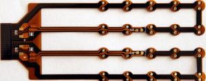
Single-sided and double-sided PCBs both use an insulating substrate, but the key difference is the number of primary copper layers available for routing.
A single-sided PCB has one primary copper layer, while a double-sided PCB has copper on both sides of the dielectric substrate.
| Feature | Single-Sided PCB | Double-Sided PCB |
|---|---|---|
| Copper routing layers | One | Two |
| Routing density | Low | Higher |
| Design complexity | Low | Moderate |
| Manufacturing complexity | Lower | Higher |
| Cost | Generally lower | Generally higher |
| Component density | Lower | Higher |
| Power/ground distribution | More limited | More flexible |
| Routing flexibility | Limited | Better |
| High-speed design | More challenging for demanding designs | More flexible |
| Typical applications | LED products, simple controls, calculators, basic power circuits | Industrial controls, automotive electronics, consumer electronics, instrumentation |
A double-sided PCB does not automatically provide better electrical performance in every application. However, the second copper layer gives designers more routing flexibility and additional options for power distribution and signal-return paths.
The correct choice depends on circuit complexity, board dimensions, cost targets, electrical performance, thermal requirements, and production volume.
Applications of Single-Sided PCBs
Single-sided PCBs remain widely used in applications where circuit complexity and routing density are relatively low.
Consumer Electronics
Examples include:
- Calculators
- Simple electronic toys
- Basic household appliances
- LED products
- Remote controls
- Simple power circuits
These products can benefit from the low cost and straightforward manufacturing of single-sided boards.
Automotive Electronics
Certain automotive subcircuits can use single-sided PCBs, particularly where circuit complexity is limited.
Examples may include:
- Basic LED control boards
- Simple lighting circuits
- Low-complexity control modules
- Auxiliary electronic circuits
The final construction must still satisfy the application’s temperature, vibration, humidity, and reliability requirements.
Industrial Electronics
Simple industrial controllers, indicator boards, sensor interfaces, and low-complexity control circuits may use single-sided PCBs.
However, demanding industrial applications may require multilayer or specialized PCB structures for improved thermal management, signal integrity, power distribution, or reliability.
LED Lighting
Single-sided metal-core PCBs are widely used for LED lighting because the metal substrate can help transfer heat away from the LED components.
The thermal design should consider LED power, thermal resistance, copper pattern, dielectric performance, heat sink interface, and ambient conditions.
Prototyping
Single-sided PCBs are also useful for prototypes and educational electronics because they are relatively simple to design and manufacture.
They allow engineers to validate basic circuit functionality before moving to more complex board structures.
How to Choose a Single-Sided PCB Manufacturer
Selecting the right manufacturer is important for achieving consistent quality and predictable production costs.
Consider the following factors:
- Manufacturing capability: Verify the manufacturer’s ability to produce your required board thickness, copper weight, hole sizes, surface finish, and tolerances.
- Material availability: Confirm that the required FR-4, CEM-1, FR-2, polyimide, or metal-core material is available.
- Quality control: Ask about AOI, electrical testing, dimensional inspection, and final inspection.
- Standards: Confirm which IPC standards and customer specifications the manufacturer can support.
- Engineering support: A capable supplier should be able to identify manufacturability issues before production.
- Production capacity: Make sure the supplier can support both prototype and volume requirements when necessary.
- Lead time: Evaluate actual production lead time rather than relying only on advertised turnaround times.
- Packaging and logistics: Proper packaging helps protect PCBs from moisture, contamination, and mechanical damage during transportation.
- Cost: Compare total manufacturing value rather than focusing only on the lowest unit price.
Kingda Single-Sided PCB Manufacturing Support
Kingda can support custom Single-Sided PCB Manufacturing for prototypes, low-volume production, and volume applications.
Depending on project requirements, the manufacturing process can include engineering review, material selection, PCB fabrication, surface finishing, electrical testing, AOI, dimensional inspection, and final quality control.
When requesting a quotation, it is helpful to provide:
- Gerber files
- Drill files
- Board dimensions
- Copper thickness
- Finished board thickness
- Substrate material
- Surface finish
- Solder mask color
- Silkscreen requirements
- Quantity
- Applicable standards
- Delivery requirements
A complete specification allows the manufacturer to evaluate manufacturability more accurately and recommend an appropriate construction.
Conclusion
A Single-Sided PCB is one of the simplest PCB structures, but its simplicity is also its main advantage. With only one primary copper layer, it provides an economical solution for low-density electronic circuits where advanced multilayer routing is unnecessary.
Its major benefits include simple design, relatively low manufacturing cost, straightforward inspection, easy troubleshooting, and suitability for high-volume production. At the same time, its single routing layer creates limitations in routing density, power distribution, grounding, thermal management, and demanding high-speed applications.
The decision to use a single-sided, double-sided, or multilayer PCB should therefore be based on the actual electrical, mechanical, thermal, space, reliability, and cost requirements of the product.
With appropriate material selection, careful PCB Design, controlled PCB Manufacturing, and comprehensive quality testing, single-sided PCBs can provide a reliable and cost-effective foundation for many electronic products.