Power PCB Design & PCB Manufacturing: Materials, Applications, Manufacturing Process & Design Guide
Electricity is the essential driving force behind modern electronics. Without a reliable power supply, no electronic device can operate properly. When supplying power to an electronic system, engineers must ensure that voltage and current remain within the acceptable operating range of every component.
Electrical power can exist in many forms, but in basic electrical engineering, power is commonly expressed by the formula P = V × I, where P represents power, V represents voltage, and I represents current. In modern electronics, this power must be efficiently controlled, converted, distributed, and managed. This is where the Power PCB becomes essential.
Unlike a conventional printed circuit board designed primarily for low-power signal processing, a power PCB is engineered to handle significantly higher current, voltage, and thermal loads. Proper PCB Design is essential for preventing excessive voltage drop, overheating, electrical breakdown, and premature component failure.
From electric vehicle inverters and solar charge controllers to industrial motor drives, power supplies, energy-storage systems, and industrial equipment, Power PCB Manufacturing provides the electrical foundation that keeps modern electrified systems operating reliably.
This guide explores the fundamentals of power PCBs, including their structure, characteristics, materials, stackup, thermal management, manufacturing process, design considerations, applications, challenges, and key factors to consider when selecting a power PCB manufacturer.
What Is a Power PCB?
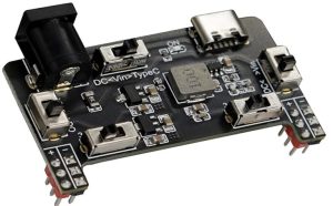
A Power PCB is a printed circuit board specifically designed to distribute, control, convert, or manage electrical power within an electronic system.
It provides both the physical platform for mounting components and the conductive pathways required to transfer electrical energy between those components.
Depending on the application, a power PCB may contain:
- Power MOSFETs
- IGBTs
- Power transistors
- Rectifiers and diodes
- Voltage regulators
- DC/DC converter circuits
- AC/DC conversion circuits
- Inductors
- Transformers
- Capacitors
- Fuses
- Power connectors
- Current and voltage sensors
- Heat sinks and thermal interfaces
Each component performs a specific function within the power-conversion or power-distribution system.
For example, MOSFETs or IGBTs can be used for high-speed switching, voltage regulators maintain a stable output voltage, capacitors store and release electrical energy, and inductors help smooth current and reduce ripple.
Thermal-management structures such as copper planes, thermal vias, heat spreaders, and heat sinks help remove heat generated during operation.
A power PCB connector provides a reliable electrical interface between the PCB and external power sources or loads. Depending on the system, these connectors may need to support high current, high voltage, repeated mating cycles, vibration, and elevated temperatures.
Therefore, a power PCB is much more than a board that connects components. It is an integral part of the system’s electrical, thermal, and mechanical architecture.
Power PCB vs. Standard PCB
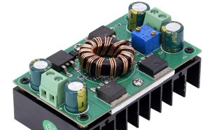
Power PCBs and standard PCBs share the same basic printed-circuit-board manufacturing principles, but their design priorities are significantly different.
The most important differences involve current capacity, copper thickness, thermal management, component selection, electrical isolation, and mechanical reliability.
| Parameter | Power PCB | Standard PCB |
|---|---|---|
| Primary function | Controls, converts, distributes, or manages electrical power | Connects electronic components and carries signals and power |
| Current capacity | Designed for moderate to very high current depending on application | Typically designed for lower current levels |
| Copper thickness | May use heavy copper or multiple copper layers | Commonly uses standard copper thicknesses |
| Thermal management | Critical design requirement | Depends on component power consumption |
| Component types | MOSFETs, IGBTs, regulators, inductors, transformers, power connectors, etc. | ICs, sensors, memory devices, passive components, connectors, etc. |
| Trace design | Wide traces, copper pours, planes, and optimized current paths | Trace geometry depends primarily on signal and current requirements |
| Electrical isolation | Often requires careful creepage and clearance design | Usually less demanding for low-voltage applications |
| Mechanical requirements | May require enhanced structural and thermal robustness | Depends on application |
| Typical applications | Power supplies, inverters, motor drives, EV systems, industrial equipment | Consumer electronics, control systems, communications, computing |
The difference is therefore not simply whether a PCB carries electrical power. Almost every PCB carries some power. A Power PCB is distinguished by the amount of power it must safely handle and the degree of electrical, thermal, and mechanical control required.
Key Characteristics of Power PCBs
A power PCB is designed around several fundamental requirements that distinguish it from conventional circuit boards.
High Current-Carrying Capacity
Power PCBs must safely carry high currents without excessive voltage drop or temperature rise.
Higher current increases resistive power loss according to:
P = I²R
As current increases, even a relatively small resistance can generate significant heat. Therefore, power PCB traces and copper planes are often made wider and thicker.
Heavy copper, copper pours, parallel copper paths, and multiple layers may be used to increase current-carrying capacity.
Thermal Management
Heat is one of the most important challenges in power electronics.
Power semiconductors, inductors, transformers, resistors, and other components can generate substantial heat. If this heat is not effectively removed, component temperature can exceed the allowable operating range.
Thermal-management techniques may include:
- Thermal vias
- Large copper planes
- Copper heat spreaders
- Heat sinks
- Metal-core PCB structures
- Thermally conductive interface materials
- Optimized component placement
- Forced-air or liquid cooling at the system level
EMI and Noise Control
Power electronics frequently involve high-speed switching. Rapid changes in voltage and current can generate electromagnetic interference (EMI).
A well-designed Power PCB should minimize unnecessary current-loop area and provide controlled return paths.
Ground planes, appropriate decoupling, filtering, shielding, and optimized switching-node layouts can all contribute to better electromagnetic compatibility (EMC).
Multilayer Construction
Multilayer construction can provide dedicated power and ground planes while separating sensitive signal circuitry from high-current switching sections.
A properly engineered multilayer stackup can reduce parasitic inductance, improve current distribution, enhance thermal performance, and help control EMI.
High Dielectric Strength
High-voltage power boards require appropriate insulation between conductive structures.
The dielectric system must withstand the required electrical stress without breakdown. Designers must also consider creepage and clearance distances, operating voltage, pollution level, environmental conditions, and applicable safety requirements.
Robust Mechanical Structure
Power electronics can experience significant thermal cycling, vibration, mechanical stress, and component weight.
A robust PCB structure helps maintain reliable solder joints, plated through-holes, connectors, and mechanical interfaces throughout the product’s operating life.
Wide Traces and Large Copper Areas
High-current PCB layouts commonly use wider traces and larger copper areas.
Increasing copper cross-sectional area reduces resistance and can improve current distribution and thermal dissipation.
However, wider traces alone do not guarantee adequate current capacity. Engineers must consider copper thickness, temperature rise, trace geometry, layer configuration, via capacity, and the actual operating environment.
Power PCB Assembly Considerations
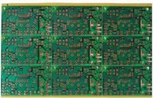
Power PCB Assembly requires careful coordination between electrical design, thermal design, component placement, and manufacturing processes.
Thermal Management
High-power components should be positioned so that heat can efficiently travel from the component into the PCB and then into the broader thermal-management system.
Thermal vias can transfer heat from component pads to internal or bottom copper planes. Heat sinks or thermal interface materials may be added when required.
Trace Width and Copper Weight
High-current paths should generally use sufficiently wide conductors and appropriate copper thickness.
Heavy copper in the range of 2–6 oz or more may be used in demanding applications, depending on the current requirement and thermal constraints.
However, copper thickness should not be selected solely according to current. Engineers should evaluate allowable temperature rise, conductor length, ambient temperature, PCB structure, and manufacturing capability.
Component Placement
Power components should be strategically positioned to minimize high-current loop areas and unnecessary interconnect length.
Switching devices, gate drivers, inductors, capacitors, and power connectors should be arranged according to the current path and switching topology.
Heat-sensitive components should also be kept away from major heat sources whenever possible.
Power and Ground Planes
Dedicated power and ground structures can provide low-impedance current paths and reduce voltage drop.
In high-speed switching applications, minimizing parasitic inductance is especially important because parasitic inductance can contribute to voltage spikes and EMI.
Materials Used in Power PCB Manufacturing
Selecting the appropriate material is fundamental to reliable Power PCB Manufacturing.
Heavy Copper
Copper thickness is one of the most important factors determining the current-carrying capability of a power PCB.
Standard PCB copper may be insufficient for high-current applications. Heavy-copper construction can provide larger conductive cross-sections and improve both electrical and thermal performance.
Depending on the application, copper thicknesses of 2 oz, 3 oz, 4 oz, 6 oz, or significantly higher may be specified.
FR-4
FR-4 remains one of the most widely used PCB substrate materials.
It provides a balance of electrical insulation, mechanical strength, processability, and cost.
FR-4 can be suitable for many low- and medium-power applications. However, high-power designs may require additional thermal-management structures or alternative materials when the thermal requirements exceed the capabilities of a conventional FR-4 construction.
Dielectric Materials
The dielectric layers provide electrical insulation between conductive layers.
For power PCBs, dielectric selection should consider:
- Dielectric strength
- Thermal resistance
- Glass-transition temperature
- Coefficient of thermal expansion
- Moisture resistance
- Thickness tolerance
- Mechanical stability
Aluminum and Metal-Core Structures
Metal-core PCBs can provide improved thermal conduction compared with conventional PCB constructions.
Aluminum-core PCBs are commonly used in applications where heat needs to be transferred efficiently from components to a heat-spreading metal structure.
Depending on the design, copper-core or other thermally optimized constructions may also be considered.
Power PCB Manufacturing Process
The Power PCB Manufacturing process transforms the PCB design data into a physical circuit board capable of handling the required electrical and thermal loads.
1. PCB Design and Engineering Review
The manufacturing process begins with the PCB design.
EDA software is used to create the schematic, layout, stackup, and manufacturing documentation.
Typical manufacturing files may include:
- Gerber files
- Drill files
- Pick-and-place files
- Fabrication drawings
- Stackup information
- Bill of materials (BOM)
- Assembly drawings
Before production, the design should undergo DFM analysis to identify potential manufacturing problems.
2. Material Preparation
The manufacturer selects the required laminate, copper foil, dielectric materials, and other construction materials according to the approved stackup.
For high-current applications, copper thickness is especially important.
3. Inner-Layer Imaging
For multilayer boards, circuit patterns are transferred onto the inner copper layers through imaging processes.
The resulting patterns define power planes, ground planes, signal paths, and other conductive structures.
4. Etching
Unwanted copper is chemically removed to create the required circuit patterns.
For heavy-copper PCBs, process control is particularly important because thicker copper requires appropriate etching parameters to achieve accurate trace geometry.
5. Layer Stacking and Lamination
The individual layers are precisely aligned and laminated under controlled heat and pressure.
Correct registration is essential because misalignment can affect vias, pads, clearances, and electrical performance.
6. Drilling
CNC mechanical drilling or laser drilling can be used to create holes required for component mounting and interlayer connections.
Power PCBs may require large numbers of thermal vias or high-current vias. Their dimensions and plating quality must be sufficient for the expected electrical and thermal loads.
7. Copper Plating
Copper is deposited inside the drilled holes to establish electrical connections between PCB layers.
For high-current applications, plated-hole reliability is particularly important because excessive current density or thermal cycling can stress the interconnections.
8. Solder Mask and Silkscreen
A solder mask is applied to protect exposed copper and reduce the risk of solder bridging.
Silkscreen is used to identify components, polarity marks, reference designators, connectors, and other assembly information.
9. Surface Finish
Common surface finishes include ENIG and HASL.
The appropriate finish depends on component requirements, soldering process, reliability requirements, pad geometry, and application environment.
10. Inspection and Testing
Power PCBs should undergo appropriate inspection before shipment.
Depending on the project, testing may include:
- AOI
- Electrical testing
- X-ray inspection
- Microsection analysis
- Dimensional inspection
- Copper-thickness verification
- Thermal testing
- Impedance testing where applicable
- Solderability testing
For demanding power applications, Kingda can establish inspection and quality-control procedures according to customer specifications and product requirements.
Power PCB Design Guidelines
Before starting a PCB Design project for a high-power application, engineers should consider electrical, thermal, mechanical, and manufacturing requirements simultaneously.
Minimize High-Current Path Length
High-current paths should generally be as short as practical.
Shorter paths reduce resistance and parasitic inductance, which can improve efficiency and reduce unwanted voltage spikes.
This is particularly important in high-frequency switching converters and inverter circuits.
Increase Conductor Width
Increasing conductor width reduces resistance and current density.
For very high-current applications, designers may use copper pours, multiple parallel layers, heavy copper, or busbar structures rather than relying on a single narrow trace.
Optimize Switching Loops
The high-current switching loop should be kept compact.
Large loop areas can increase parasitic inductance and electromagnetic radiation. Careful placement of switching devices and decoupling capacitors can significantly improve power-stage performance.
Place Decoupling Capacitors Correctly
Decoupling capacitors should be placed close to the relevant power pins or switching devices.
The physical connection between the capacitor and the switching loop should be kept short and low impedance.
Optimize Thermal Paths
Thermal vias should be placed beneath or near heat-generating components when appropriate.
Large copper areas can distribute heat across the PCB, while metal-core structures or external heat sinks can provide additional thermal-management capability.
Separate Sensitive and Noisy Circuits
Sensitive analog, sensing, and communication circuits should be appropriately separated from high-current switching sections.
This does not necessarily mean completely isolating every circuit with separate grounds. Instead, the grounding and return-current strategy should be designed according to the actual circuit topology.
Design Appropriate Creepage and Clearance
For high-voltage power PCBs, creepage and clearance must be designed according to the applicable safety standards and operating environment.
The required distances depend on factors such as working voltage, insulation category, pollution degree, altitude, and material characteristics.
Perform Electrical and Thermal Simulation
Simulation tools can help engineers identify problems before fabrication.
Depending on the design, engineers may perform:
- Power-integrity analysis
- Thermal simulation
- SPICE simulation
- Electromagnetic analysis
- Voltage-drop analysis
- Current-density analysis
Tools such as Altium Designer and PSpice can be incorporated into the development workflow depending on project requirements.
Limitations and Challenges of Power PCBs
Power PCB development presents several technical challenges.
Heat Generation
High current produces resistive losses according to I²R.
Switching losses and component losses can further increase temperature.
Without adequate thermal management, excessive temperature can reduce efficiency and shorten component life.
Large Physical Size
High-power components, heat sinks, transformers, inductors, and high-current connectors can increase the overall size and weight of the system.
This can make miniaturization more difficult.
Higher Manufacturing Cost
Heavy copper, advanced thermal structures, specialized materials, and tighter manufacturing tolerances can increase PCB fabrication costs.
Therefore, engineers should balance electrical performance with manufacturability during the initial design stage.
EMI from High-Speed Switching
High-frequency switching creates rapidly changing voltage and current waveforms.
Poor layout can increase EMI, ringing, overshoot, and unwanted coupling between circuits.
Thermal Cycling and Reliability
Repeated heating and cooling can cause mechanical stress because different PCB materials and components expand at different rates.
Over time, thermal cycling can affect solder joints, vias, component connections, and laminate structures.
Manufacturing Complexity
Heavy-copper and high-power multilayer PCBs can require more demanding etching, lamination, drilling, plating, and inspection processes than standard PCBs.
This makes manufacturer experience an important consideration.
Common Applications of Power PCBs
Power PCBs are used in a broad range of industries where electrical energy must be converted, controlled, or distributed.
Power Supplies
Power PCBs are widely used in AC/DC converters, DC/DC converters, switching power supplies, battery chargers, and industrial power supplies.
Automotive Electronics
Modern vehicles contain numerous high-power electronic systems.
Applications include:
- EV inverters
- On-board chargers
- DC/DC converters
- Battery-management systems
- Electric motor controllers
- Power distribution units
- Automotive lighting systems
Industrial Motor Drives
Industrial automation systems require power electronics to control motors, pumps, fans, compressors, and other equipment.
Power PCBs provide the switching and control infrastructure required by these systems.
Renewable Energy
Solar inverters, energy-storage systems, wind-power electronics, and battery systems rely on power conversion and management circuits.
Power PCBs are essential for controlling energy flow between generation, storage, and loads.
Consumer Electronics
High-power consumer devices can also contain specialized power PCBs.
Examples include power amplifiers, high-performance computing equipment, appliances, and smart-home power-management systems.
Aerospace and Defense
Aerospace and defense equipment often requires highly reliable power-conversion and power-distribution electronics.
Power PCBs can be used in radar power systems, satellite power electronics, avionics, communication systems, and other mission-critical equipment.
Medical Equipment
Medical devices require stable and reliable power.
Power PCBs can be found in equipment such as imaging systems, medical power supplies, surgical equipment, patient-monitoring systems, and laboratory instruments.
How to Choose the Right Power PCB Manufacturer
Choosing the right Power PCB Manufacturer can have a direct impact on electrical performance, reliability, production cost, and delivery time.
1. Evaluate High-Current PCB Experience
First, determine whether the manufacturer has practical experience producing high-current and heavy-copper PCBs.
Ask about previous experience with copper thickness, multilayer structures, high-current vias, thermal management, and high-power applications.
2. Verify Manufacturing Capabilities
Confirm whether the supplier can manufacture the required:
- Copper thickness
- Number of layers
- Board thickness
- Minimum trace and spacing
- Via structures
- Surface finish
- Material system
- Thermal structures
These capabilities should match the actual requirements of your design.
3. Examine Quality-Control Procedures
A reliable manufacturer should have appropriate inspection and testing capabilities.
Ask about AOI, electrical testing, X-ray inspection, microsection analysis, copper-thickness measurement, and other relevant quality-control processes.
4. Review DFM and Engineering Support
Good manufacturing support should begin before production.
An experienced supplier can identify issues related to trace width, copper distribution, thermal structures, drilling, plating, lamination, and component assembly before they become production problems.
5. Check Certifications
Depending on the target market and application, relevant certifications and standards may include ISO 9001 and applicable IPC requirements.
Automotive, medical, aerospace, and other specialized applications may require additional standards or customer-specific qualifications.
6. Consider Production Capacity
The manufacturer should be able to support your required prototype quantities, production volumes, lead times, and quality requirements.
A suitable supplier should also have a stable process for maintaining consistency between prototype and mass production.
7. Evaluate Technical Communication
Power PCB projects often involve detailed discussions regarding stackup, copper thickness, thermal performance, electrical isolation, and manufacturing tolerances.
Clear communication between the engineering team and manufacturer can reduce design iterations and production risks.
Kingda provides PCB manufacturing and engineering support for customers requiring standard, multilayer, heavy-copper, and other specialized PCB solutions.
Why Power PCB Design and Manufacturing Matter
The performance of a power electronic system depends heavily on the quality of its PCB architecture.
A poorly designed power PCB can experience:
- Excessive voltage drop
- High temperature rise
- EMI problems
- Switching noise
- Voltage overshoot
- Solder-joint stress
- Component overheating
- Reduced efficiency
- Premature failure
A properly engineered power PCB, by contrast, provides controlled current paths, efficient thermal transfer, reliable electrical insulation, and improved mechanical stability.
This is why PCB Design and PCB Manufacturing should not be treated as separate stages. The design must take manufacturing capabilities into account from the beginning.
Future Trends in Power PCB Technology
The increasing electrification of transportation, energy systems, industrial automation, and computing is creating new requirements for power electronics.
Several trends are shaping the development of power PCBs.
Higher Power Density
Modern systems increasingly need to deliver more power within smaller physical spaces.
This places greater demands on copper utilization, thermal management, component integration, and PCB layout.
Wide-Bandgap Semiconductors
Gallium nitride (GaN) and silicon carbide (SiC) power devices enable high-frequency and high-efficiency switching in many applications.
However, their fast switching behavior also makes PCB parasitics and layout optimization increasingly important.
Advanced Thermal Management
As power density increases, traditional cooling approaches may not always be sufficient.
Advanced copper structures, metal-core PCBs, embedded thermal solutions, heat spreaders, and improved interface materials are becoming increasingly important.
Electrification and Energy Storage
Electric vehicles, battery energy-storage systems, renewable-energy installations, and charging infrastructure are driving continued demand for high-current and high-reliability power electronics.
Integration of Power and Control
Modern power systems increasingly combine power stages, sensing circuits, communication interfaces, and digital control within compact assemblies.
This creates new challenges in separating high-power switching noise from sensitive control and communication signals.
Conclusion
The Power PCB is a fundamental component of modern power electronics. It provides the conductive paths, component interfaces, electrical insulation, thermal structures, and mechanical foundation required to safely control and distribute electrical energy.
Unlike standard PCBs, power boards must often handle high current, elevated temperatures, rapid switching, and high electrical stress. As a result, successful Power PCB Design requires careful consideration of copper thickness, trace width, current density, thermal management, grounding, EMI control, creepage and clearance, component placement, and PCB stackup.
At the manufacturing stage, material selection, heavy-copper processing, lamination, drilling, plating, surface finishing, inspection, and testing all contribute to final board reliability.
With the rapid growth of electric vehicles, renewable energy, energy storage, industrial automation, high-performance computing, and other electrification technologies, the role of Power PCB Manufacturing will become increasingly important.
For companies developing high-power electronic products, working with an experienced manufacturing partner such as Kingda can help bridge the gap between power-system requirements, manufacturable PCB design, and consistent production quality.