PCB Edge Connectors: PCB Design, PCB Manufacturing & Card Edge Connector Guide
PCB connectors are available in a wide range of sizes, shapes, materials, and configurations. They provide reliable electrical and mechanical interfaces between circuit boards, cables, components, and external systems. Among the many connector technologies used in modern electronics, PCB Edge Connectors are particularly important for applications that require a direct and repeatable connection between a PCB and a mating socket.
Also known as card-edge connectors, these interfaces are widely used in computers, telecommunications equipment, industrial electronics, storage devices, and other systems that require removable circuit boards or high-density signal connections.
This article provides a technical overview of PCB Edge Connectors, including their construction, connection methods, common types, selection criteria, manufacturing considerations, edge beveling, and current technology trends.
What Is a PCB Edge Connector?
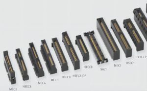
A PCB Edge Connector is a connector interface located directly along the edge of a printed circuit board. Instead of using a separate male connector mounted on the PCB, the exposed conductive contacts along the board edge function as the mating interface.
The PCB is inserted into a corresponding female connector or socket. When the board is fully inserted, spring contacts inside the connector press against the exposed PCB contacts to establish electrical continuity.
This approach is commonly used for removable expansion cards and modules. Typical examples include PCI and PCI Express expansion cards, memory modules, storage interfaces, and various industrial control boards.
The exposed contact area is often called a gold finger PCB because the contacts typically have a gold surface finish designed for repeated mating and improved contact reliability.
Gold is widely used because it provides good electrical conductivity and corrosion resistance. Depending on the application and manufacturing requirements, different gold-plating structures may be specified.
It is important to distinguish between ENIG and edge-contact hard gold. ENIG deposits a relatively thin immersion-gold layer over electroless nickel and is primarily used as a general PCB surface finish. Card-edge contacts that must withstand repeated insertion and removal commonly use a harder electroplated gold finish over nickel, often referred to as hard gold or selective gold plating.
Therefore, ENIG should not automatically be treated as equivalent to a hard-gold edge connector.
How Do PCB Edge Connectors Connect?
Card-edge interfaces can be integrated into a larger electronic system in several ways. The appropriate configuration depends on the mechanical architecture, signal requirements, available space, and serviceability requirements.
Board-to-Board Connections
Board-to-board connectors provide a direct electrical interface between two PCBs. They are widely used in compact electronic equipment where boards must communicate with one another without additional cabling.
These connections can support high-density and high-speed signals, but the mechanical structure must be carefully designed when the system is exposed to vibration, shock, or repeated mechanical stress.
Board-to-Wire Connections
Board-to-wire connections connect a PCB to external wires or cable assemblies. They provide greater flexibility in system architecture because cables can be routed around mechanical structures and connected to remote components.
For card-edge applications, the connector housing and contact arrangement must be selected according to the required orientation, current rating, signal integrity, and available space.
Wire-to-Wire Connections
Wire-to-wire connectors join two cable assemblies without directly mounting the connector to a PCB. They are useful when flexibility and serviceability are important.
However, connector selection for higher-power applications requires careful consideration of contact resistance, current rating, temperature rise, insulation system, and mechanical reliability.
Common Types of PCB Edge Connectors
Different electronic systems use different card-edge interfaces. Their mechanical dimensions, contact arrangement, keying, pitch, electrical specifications, and mating requirements can vary significantly.
PCI and PCI Express Edge Connectors
PCI and PCI Express expansion interfaces are among the best-known examples of card-edge technology.
A graphics card, network adapter, sound card, or other expansion board can use exposed edge contacts that mate directly with a slot on the motherboard.
PCI Express has become particularly important for high-speed data communication between processors, storage devices, graphics hardware, and other peripherals.
For these applications, PCB Design must account for controlled impedance, differential-pair routing, return paths, insertion loss, crosstalk, and connector discontinuities.
The connector itself is therefore only one part of the overall high-speed channel.
Mobile Device and Battery Interfaces
Compact electronic devices can use edge-style contacts or board-edge interfaces for battery, module, display, or other internal connections.
Because portable products have strict space and mechanical requirements, connector designs often emphasize compact dimensions, reliable contact force, low profile, and resistance to repeated assembly cycles.
SIM Card Connectors
A SIM card interface is another familiar example of a removable card interface. The SIM card contains conductive contacts that mate with spring contacts in the card socket.
Although its mechanical construction differs from a conventional expansion-card slot, the underlying concept is similar: exposed contacts on a removable card establish an electrical connection with contacts in a receptacle.
Display Interfaces
Display systems use various connector technologies to transmit video and control signals. HDMI is a familiar example in consumer electronics, although it is generally implemented as a dedicated connector rather than a conventional PCB card-edge slot.
Within electronic equipment, PCB-mounted display connectors must be designed around signal speed, mechanical retention, shielding, impedance control, and connector durability.
Eurocard Connectors
Eurocard connectors are used extensively in industrial and telecommunications equipment. They are associated with standards such as DIN 41612 and IEC 60603-2 and can provide high-density interconnections between circuit boards and backplanes.
Different configurations are available for different contact arrangements, signal requirements, and mechanical architectures.
M.2 Card-Edge Interfaces
M.2 is a compact interface commonly used for SSDs, wireless modules, and other expansion devices.
M.2 cards use an edge connector with a specific keying arrangement. The key position determines mechanical compatibility and helps prevent installation of an incompatible module.
M.2 modules are identified by physical dimensions such as width and length, with common module sizes including 2230, 2242, 2260, and 2280.
When designing an M.2 interface, engineers must consider not only the connector footprint but also the mechanical clearance, mounting hole, keying, high-speed routing, power delivery, and thermal requirements.
Key Factors for Selecting a PCB Edge Connector
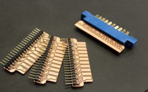
Selecting a card-edge connector requires more than checking the number of contacts. The electrical, mechanical, environmental, and manufacturing requirements should all be considered.
Electrical Connectivity
The connector must support the required voltage, current, frequency, and signaling method.
For high-speed interfaces, engineers should evaluate:
- Contact resistance
- Characteristic impedance
- Insertion loss
- Return loss
- Crosstalk
- Differential-pair performance
- Signal discontinuities
- Ground and return-path design
A connector with adequate contact count may still be unsuitable if its electrical characteristics do not support the target data rate.
Signal Integrity
Modern PCBs often carry mixed signal types, including DC power, low-speed digital signals, high-speed differential signals, and sensitive analog signals.
A poorly selected or poorly designed connector interface can introduce impedance discontinuities and additional parasitic effects.
During PCB Design, engineers should therefore consider the entire signal path, including the PCB trace, connector contact, mating connector, vias, reference planes, and receiving device.
For high-speed systems, simulation and measurement such as TDR or VNA-based characterization may be appropriate depending on the interface requirements.
Mechanical Durability
Card-edge connectors may experience insertion and removal cycles, vibration, shock, thermal expansion, and mechanical stress.
Important specifications include:
- Mating-cycle rating
- Contact normal force
- Retention force
- Housing strength
- Contact geometry
- PCB thickness tolerance
- Vibration resistance
- Shock resistance
The selected connector should be compatible with the mechanical strength and dimensional tolerances of the PCB.
Contact Material and Surface Finish
The contact material and plating system have a major influence on connector reliability.
Gold is frequently used for card-edge contacts because of its corrosion resistance and stable contact properties. For applications involving repeated mating cycles, hard electroplated gold is generally more appropriate than a thin immersion-gold finish intended for soldering surfaces.
The plating thickness, nickel underlayer, contact geometry, and mating-cycle requirement should all be specified according to the application.
Environmental Requirements
Industrial, automotive, medical, telecommunications, and consumer products can have very different environmental requirements.
Depending on the application, the connector may need to withstand:
- High or low temperatures
- Humidity
- Dust
- Vibration
- Shock
- Corrosive environments
- Repeated mating
- Chemical exposure
Material selection should also comply with applicable environmental and regulatory requirements, such as RoHS where required.
PCB Edge Connector Design Considerations
Reliable card-edge performance begins during PCB layout rather than after manufacturing.
Contact Geometry
The contact length, width, spacing, and position must match the mating connector specification.
The PCB manufacturer must receive accurate fabrication data defining the edge contacts, board thickness, plating requirements, and mechanical dimensions.
Contact Pitch
As electronic products become smaller and more functionally integrated, connector pitch continues to decrease.
Fine-pitch card-edge interfaces require tighter control of:
- Copper geometry
- Solder mask clearance
- Contact spacing
- Etching accuracy
- Board thickness
- Plating
- Edge dimensions
Manufacturing tolerances become increasingly important as contact spacing decreases.
Board Thickness
The PCB thickness must be compatible with the connector slot.
An incorrect board thickness can result in excessive insertion force, poor contact pressure, mechanical damage, or an unreliable electrical connection.
Therefore, the nominal PCB thickness and allowable tolerance should be defined before selecting the connector.
Edge Clearance
Copper traces and other structures near the PCB edge must maintain sufficient clearance from the board outline.
This is particularly important when the board is inserted into a metal connector housing or another mechanically constrained structure.
Edge Plating
Edge plating and selective plating requirements should be clearly defined in the fabrication documentation.
For card-edge contacts, the manufacturer may need to apply nickel and hard gold selectively to the contact area rather than plating the entire board with the same finish.
This approach can improve performance while controlling manufacturing cost.
How Are PCB Edge Connectors Manufactured?
A card-edge interface is not simply a connector mounted onto the PCB. The PCB itself becomes part of the mating interface.
The typical manufacturing process can include:
- PCB material preparation
- Inner-layer fabrication for multilayer boards
- Lamination
- Drilling
- Copper plating
- Circuit imaging and etching
- Solder mask application
- Surface finishing
- Edge-contact plating
- PCB routing and profiling
- Edge beveling
- Electrical testing
- Dimensional inspection
- Final quality inspection
The exact process depends on the PCB construction, contact plating requirements, board thickness, layer count, and connector specification.
For high-reliability applications, PCB Manufacturing should maintain tight control over contact dimensions, plating thickness, board profile, and edge geometry.
PCB Edge Beveling and Chamfering
One of the most important mechanical features of a card-edge PCB is the beveled edge.
A PCB that is repeatedly inserted into a connector normally requires a controlled lead-in geometry. This allows the board to enter the connector more smoothly and reduces the risk of damaging the contacts.
The process is commonly described as PCB edge beveling or chamfering.
What Is a PCB Edge Bevel?
A bevel is an angled surface created by removing material from an edge.
For card-edge PCBs, the bevel is typically applied to the insertion edge so that the board enters the connector gradually rather than presenting a sharp 90-degree edge.
The exact bevel angle and dimensions must be specified according to the mating connector.
A common bevel angle is approximately 30°, but this should never be treated as a universal value. PCI/PCIe and other interfaces may have specific mechanical requirements defined by the relevant specification.
Beveling vs. Chamfering
The terms bevel and chamfer are sometimes used interchangeably, but they describe different geometric concepts.
A bevel generally refers to an angled surface formed along an edge. The angle can vary according to the mechanical requirement.
A chamfer is a deliberately cut-away edge or corner, commonly used to eliminate a sharp edge and improve mechanical assembly.
For PCB card-edge applications, manufacturers typically follow the dimensions and geometry specified by the connector or interface standard rather than relying on a generic bevel or chamfer value.
This distinction is important because the insertion angle, depth, board thickness, and contact geometry all influence connector compatibility.
Why Is PCB Edge Beveling Important?
A properly manufactured edge bevel provides several practical benefits:
- Smoother insertion: The angled edge guides the PCB into the connector.
- Reduced contact damage: The connector contacts are less likely to encounter an abrupt board edge.
- Improved mechanical integration: The board can engage more smoothly with the connector housing.
- Better repeatability: Consistent edge geometry supports reliable insertion across production batches.
- Reduced assembly stress: A controlled lead-in geometry can reduce unnecessary mechanical force.
The bevel must be manufactured consistently. Excessive material removal can reduce the contact area or alter the intended mechanical position of the edge contacts.
PCB Manufacturing Requirements for Card-Edge Contacts
Because the PCB edge becomes part of the connector system, several manufacturing parameters deserve particular attention.
Plating Thickness
The required gold thickness depends on the mating-cycle requirement and connector specification.
Hard-gold contacts generally require controlled electroplated gold over a nickel layer. The plating should be limited to the required contact area when selective plating is specified.
Edge Dimensions
The PCB profile must meet the mechanical tolerance specified by the connector manufacturer.
Important dimensions include:
- Board thickness
- Edge length
- Bevel angle
- Bevel depth
- Contact width
- Contact pitch
- Contact-to-edge distance
- Overall PCB dimensions
Surface Quality
The edge-contact area should be free from defects that could compromise electrical contact or mechanical insertion.
Manufacturing inspection should check for:
- Scratches
- Plating voids
- Peeling
- Burrs
- Excessive roughness
- Dimensional deviations
- Contamination
Electrical Testing
Electrical testing can verify circuit continuity and isolation, while additional high-speed characterization may be required for demanding interfaces.
For a complete production program, electrical testing should be combined with dimensional inspection and visual inspection.
Technology Trends in PCB Edge Connectors
The development of electronic products continues to increase the requirements placed on card-edge interfaces.
Higher data rates require better control of impedance, crosstalk, insertion loss, and return loss. At the same time, smaller products require higher contact density and tighter mechanical tolerances.
Modern edge-connector solutions increasingly focus on:
- Higher contact density
- Smaller pitch
- Higher data rates
- Improved signal integrity
- More precise plating
- Lower contact resistance
- Improved mechanical retention
- Smaller connector footprints
- More reliable materials
- Better thermal performance
For advanced PCB Design, connector selection should occur early in the design process. Waiting until the final layout stage can create problems with routing space, impedance control, mechanical clearance, and manufacturing tolerances.
Applications of PCB Edge Connectors
Card-edge interfaces are used across a wide range of electronic products.
Common applications include:
| Application | Typical Use |
|---|---|
| Computers | Expansion cards, graphics cards, storage interfaces |
| Telecommunications | Line cards, backplanes, communication modules |
| Industrial Electronics | Control modules and replaceable circuit boards |
| Data Centers | High-speed expansion and storage systems |
| Automotive Electronics | Modular control and communication systems |
| Medical Electronics | Replaceable electronic modules |
| Consumer Electronics | Memory, storage, and removable modules |
| Test Equipment | Plug-in measurement and interface boards |
The exact connector technology depends on the required electrical performance, mechanical structure, environmental conditions, and service requirements.
How to Choose the Right PCB Edge Connector
A systematic selection process can help engineers avoid compatibility and reliability problems.
Step 1: Define the Electrical Requirements
Determine voltage, current, frequency, data rate, impedance, and signal type.
Step 2: Define the Mechanical Requirements
Confirm board thickness, connector dimensions, contact pitch, keying, mounting method, insertion direction, and required mating cycles.
Step 3: Select the Contact Material
Choose the appropriate plating structure based on contact resistance, corrosion resistance, mating frequency, and environmental conditions.
Step 4: Verify PCB Design Compatibility
Check contact dimensions, routing space, reference planes, impedance requirements, edge clearance, and board profile.
Step 5: Confirm Manufacturing Capability
The PCB manufacturer should be able to control edge plating, bevel dimensions, contact geometry, board thickness, and overall dimensional tolerances.
Step 6: Perform Prototype and Reliability Testing
Prototype testing should verify insertion force, mating performance, electrical continuity, signal integrity, and mechanical durability as applicable.
Kingda PCB Edge Connector Manufacturing Support
For card-edge applications, PCB fabrication and connector compatibility must be considered as one integrated engineering problem.
Kingda supports PCB projects that require precise board dimensions, controlled copper geometry, edge-contact plating, PCB beveling, multilayer construction, and electrical testing.
For high-speed card-edge applications, the design should be reviewed from both the PCB Design and PCB Manufacturing perspectives. Signal integrity, stackup, impedance control, contact geometry, plating, mechanical tolerances, and manufacturability should be evaluated together.
This approach helps reduce prototype iterations and improves the consistency of production boards.
Conclusion
PCB Edge Connectors provide a practical interface between removable circuit boards and electronic systems. By using conductive contacts directly along the PCB edge, they can reduce connector complexity while supporting compact, high-density, and serviceable electronic designs.
However, reliable card-edge performance depends on much more than the connector itself. Contact plating, board thickness, contact pitch, signal integrity, mechanical durability, edge geometry, bevel dimensions, and manufacturing tolerances all contribute to overall performance.
For modern high-speed electronics, PCB Design and PCB Manufacturing must be coordinated from the beginning. Selecting the appropriate connector, defining the correct edge-contact structure, controlling the plating process, and maintaining precise PCB dimensions are essential steps toward achieving reliable card-edge connections.
With appropriate material selection, accurate fabrication, controlled edge beveling, and comprehensive inspection, PCB card-edge interfaces can provide a robust solution for computing, telecommunications, industrial electronics, storage, automotive, and other demanding applications.