12-Layer PCB Stackup: PCB Design, PCB Manufacturing & Layer Stackup Guide
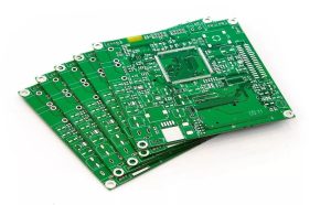
Multilayer PCBs are the backbone of modern electronic products. From smartphones and laptops to networking equipment, servers, industrial controllers, and advanced communication systems, many of today’s high-performance electronic devices rely on multilayer printed circuit boards.
A multilayer PCB can contain anywhere from four layers to dozens of conductive layers. In general, engineers try to minimize the number of PCB layers to control material and manufacturing costs. However, increasing the layer count can provide more routing space, better power distribution, improved return-path management, and greater flexibility for electromagnetic compatibility (EMC) and signal-integrity design.
A 12-Layer PCB is one such high-layer-count configuration. It provides substantially more routing and reference-plane resources than conventional 4-layer or 6-layer boards, making it suitable for complex electronic systems where space, performance, and electrical reliability are important.
This article explains the structure of a 12-Layer PCB Stackup, including its layer configuration, dielectric materials, signal and power distribution, PCB Design considerations, thermal management, EMC requirements, and PCB Manufacturing considerations.
What Is a 12-Layer PCB Stackup?
A 12-Layer PCB Stackup is a multilayer printed circuit board construction containing 12 copper layers separated by dielectric materials.
Depending on the manufacturing process, the board may contain a combination of copper-clad cores and prepreg dielectric layers. Therefore, it is more accurate to describe a 12-layer PCB as having 12 conductive copper layers rather than assuming that exactly 11 discrete dielectric sheets are always used.
The 12 copper layers can be assigned different functions, including:
- High-speed signal routing
- General-purpose signal routing
- Power distribution
- Ground/reference planes
- Analog or sensitive-signal routing
- Specialized RF or high-speed interconnects
The exact assignment depends on the electrical requirements of the product.
Unlike simpler 4-layer and 6-layer boards, a 12-layer PCB provides considerably more freedom for separating high-speed signals, power distribution, and sensitive circuits. It can also provide more opportunities for continuous reference planes and controlled-impedance routing.
However, a higher layer count does not automatically guarantee better electrical performance. The stackup must be engineered around the actual signal paths, reference planes, dielectric thicknesses, materials, manufacturing capabilities, and mechanical requirements.
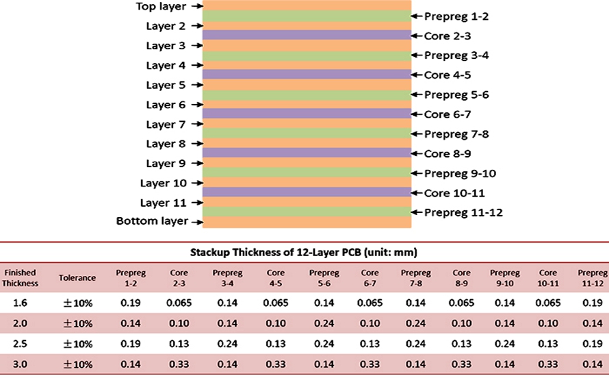
Typical 12-Layer PCB Stackup
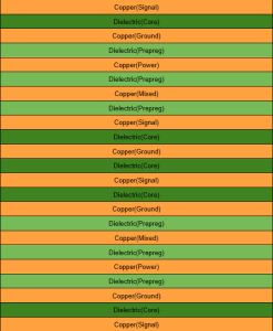
There is no single universal 12-layer stackup that is suitable for every application. A practical configuration should be created according to signal-speed requirements, power architecture, routing density, impedance targets, EMC requirements, and fabrication capabilities.
A representative 12-layer configuration could be organized as follows:
| Layer | Typical Function |
|---|---|
| L1 | Component / high-speed signal |
| L2 | Ground / reference plane |
| L3 | High-speed signal |
| L4 | General signal |
| L5 | Ground plane |
| L6 | Power plane |
| L7 | Power plane |
| L8 | Ground plane |
| L9 | General signal |
| L10 | High-speed signal |
| L11 | Ground / reference plane |
| L12 | Component / signal |
This is only an example rather than a universal recommendation. The actual stackup should be adjusted based on the required impedance, routing density, power distribution, thermal behavior, and manufacturing process.
For example, a design with several high-speed interfaces may require more dedicated signal layers and carefully positioned reference planes. A power-dense system may instead allocate additional layers to power distribution.
Copper Layers in a 12-Layer PCB
The 12 conductive layers can be divided into different functional groups.
Signal Layers
Signal layers carry electrical connections between components, connectors, ICs, and other devices.
High-speed signals should be routed on layers with well-defined reference planes and controlled dielectric geometry. This helps engineers maintain predictable impedance and provides a continuous return path.
In a complex 12-layer board, several layers can be dedicated to high-speed signals. These layers may support interfaces such as:
- PCI Express
- USB
- DDR memory
- Ethernet
- SerDes
- High-speed ADC/DAC interfaces
- RF and microwave circuits
The exact number of signal layers depends on routing density and interface requirements.
Mixed or General-Purpose Signal Layers
Not every signal requires the same level of impedance control.
General-purpose GPIO, low-speed digital signals, control lines, and other less-sensitive networks can be assigned to appropriate internal or external layers.
Separating high-speed and general-purpose routing can simplify layout and reduce unnecessary routing congestion.
Power Layers
Dedicated power planes can improve power distribution and reduce routing congestion.
A 12-layer PCB may contain multiple power domains, especially in systems that require several voltage rails.
Power planes should be positioned carefully relative to ground planes. Closely coupled power and ground planes can also provide useful high-frequency decoupling characteristics, depending on the dielectric thickness and material.
However, power-plane design should be based on actual current distribution, impedance, voltage domains, and return-current requirements rather than simply increasing the number of power layers.
Ground and Reference Planes
Ground planes provide low-impedance return paths and reference surfaces for controlled-impedance traces.
For high-speed signals, maintaining a continuous reference plane is particularly important. When a signal changes layers through a via, the return current must also transition appropriately.
Ground planes can also help reduce electromagnetic coupling between different routing regions.
However, adding more ground layers is not automatically beneficial. The effectiveness of a ground plane depends on its location, continuity, connection strategy, dielectric spacing, and relationship with the signal layers.
Dielectric Layers in a 12-Layer PCB
The dielectric structure is one of the most important parts of a 12-Layer PCB Stackup.
A multilayer PCB generally uses two primary dielectric structures: core materials and prepreg.
Prepreg
Prepreg is a resin-and-glass-fiber material used to bond copper-clad cores and other layers during lamination.
After lamination, the resin becomes part of the board’s dielectric system.
The final dielectric thickness depends on factors such as:
- Prepreg type
- Glass style
- Resin content
- Copper thickness
- Lamination pressure
- Manufacturing process
For high-speed PCB Design, dielectric thickness is particularly important because it directly affects the geometry of controlled-impedance traces.
Core Materials
A core is a rigid dielectric laminate with copper foil already bonded to one or both sides before multilayer lamination.
Core materials provide mechanical stability and contribute to the electrical structure of the PCB.
Unlike prepreg, which flows during lamination, the core has a more controlled and stable thickness.
The number of core sections in a 12-layer board depends on the chosen manufacturing stackup. It is therefore not technically accurate to assume that every 12-layer PCB must contain exactly five or six cores.
Why Is Dielectric Thickness Important?
In high-speed PCB design, dielectric thickness affects the relationship between the trace and its reference plane.
For a controlled-impedance microstrip or stripline structure, impedance depends on multiple parameters, including:
- Trace width
- Trace thickness
- Dielectric thickness
- Dielectric constant
- Reference-plane geometry
- Copper roughness
Therefore, the dielectric thickness should be finalized together with the impedance target.
If the dielectric spacing changes significantly between stackup revisions, trace dimensions may need to be recalculated.
12-Layer PCB Design Considerations
A high-layer-count PCB provides significant design flexibility, but it also introduces additional engineering challenges.
1. Define the Top and Bottom Layers
The outer layers are commonly used for component placement, connectors, and accessible routing.
High-speed signals may be routed on the outer layers when appropriate, but they should not automatically be preferred simply because they can avoid vias.
In many designs, internal stripline routing can provide better electromagnetic containment and more consistent impedance.
The decision should be based on signal-integrity, EMI, manufacturability, and component-placement requirements.
2. Plan the Stackup Before Routing
The stackup should be established before detailed routing begins.
Engineers should define:
- Layer functions
- Copper thickness
- Dielectric thickness
- Material type
- Reference planes
- Power domains
- Impedance targets
- Via structures
A well-planned stackup reduces routing changes later in the design cycle.
3. Control Impedance
High-speed interfaces often require controlled impedance.
For differential pairs, both differential impedance and the individual conductor geometry may need to be controlled.
The impedance model should account for:
- Trace width
- Trace spacing
- Copper thickness
- Dielectric constant
- Dielectric thickness
- Reference-plane distance
- Copper roughness
The final dimensions should be confirmed against the PCB manufacturer’s actual material stackup.
4. Maintain Continuous Return Paths
High-speed signals require appropriate return-current paths.
When a trace crosses from one layer to another, its return path may also need a suitable transition mechanism. Poorly managed reference-plane changes can increase loop area and contribute to EMI or signal-integrity problems.
Ground stitching vias and appropriately placed return vias can help maintain a controlled return path where required.
5. Manage Via Structures
A 12-layer PCB can require a large number of vias.
Depending on routing density and electrical requirements, designers may use:
- Through vias
- Blind vias
- Buried vias
- Microvias
- Via-in-pad structures
HDI technology can provide additional routing flexibility, but it also increases manufacturing complexity and cost.
Therefore, HDI should be used where it solves a genuine routing, size, or electrical requirement rather than simply because the PCB has a high layer count.
Material Selection for 12-Layer PCBs
Material selection has a direct effect on electrical performance, thermal behavior, reliability, and manufacturing cost.
FR-4
FR-4 remains one of the most widely used PCB laminate families and can be used for many 12-layer applications.
However, standard FR-4 is not necessarily the optimal material for every high-speed or high-frequency design.
When signal loss, dielectric stability, high-frequency performance, or demanding HDI requirements become critical, engineers may choose specialized low-loss or high-speed laminates.
High-Performance Materials
Depending on the application, high-performance materials may include products from manufacturers such as Rogers, Isola, or Panasonic.
Examples include:
- Rogers RO4350B
- Isola Tachyon series
- Panasonic Megtron series
Material selection should be based on the actual requirements for dielectric constant, dissipation factor, insertion loss, thermal performance, glass-transition temperature, coefficient of thermal expansion, reliability, and manufacturing availability.
It is also important to verify the exact material grade rather than treating an entire manufacturer or product family as having identical electrical properties.
EMC and EMI Considerations
A properly designed 12-layer stackup can provide strong EMC benefits because engineers have more freedom to position reference planes and isolate sensitive routing.
For example, a sensitive high-speed signal layer can be placed between reference planes in a stripline configuration.
This can help:
- Reduce electromagnetic radiation
- Control return-current paths
- Reduce coupling between circuits
- Improve shielding between functional regions
- Support controlled impedance
However, the stackup alone does not guarantee EMC compliance.
EMC performance also depends on:
- PCB layout
- Grounding strategy
- Return paths
- Via placement
- Component placement
- Cable interfaces
- Connector design
- Power distribution
- Enclosure design
Therefore, EMC should be considered throughout the complete PCB Design process.
Thermal Management in 12-Layer PCBs
High-layer-count PCBs are often used in compact, high-performance systems where thermal density can be significant.
Thermal management should therefore be incorporated into both the PCB stackup and layout.
Common techniques include:
Thermal Vias
Thermal vias can transfer heat from component pads or thermal regions into internal copper structures.
They are particularly useful beneath power components, processors, regulators, and other heat-generating devices when the package and assembly process permit their use.
Copper Planes
Large copper regions can distribute heat across the board.
However, copper distribution should be balanced during fabrication. Large differences in copper density between layers can affect lamination behavior and contribute to board deformation.
Thermally Conductive Materials
Specialized PCB materials can be considered when standard laminate performance is insufficient.
Material selection should be based on the actual thermal requirement rather than simply choosing a material with the highest published thermal conductivity.
External Thermal Solutions
Heat sinks, thermal interface materials, chassis structures, and forced-air cooling can complement PCB-level thermal management.
The most effective thermal solution is often a combination of component placement, copper distribution, thermal vias, PCB materials, and system-level cooling.
Cost Considerations for 12-Layer PCB Manufacturing
A 12-layer board generally costs more to manufacture than a simpler 4-layer or 6-layer PCB.
The cost increase can come from:
- Additional copper layers
- More dielectric materials
- Longer lamination processes
- More drilling operations
- Additional inspection
- More complex via structures
- Higher material costs
- Tighter manufacturing tolerances
- Controlled-impedance requirements
- Special surface finishes
- HDI processes
The use of advanced materials can further increase cost.
Copper thickness is another important factor. Heavier copper may improve current-carrying capability and thermal spreading, but it can make fine-line etching and multilayer fabrication more difficult.
PCB thickness also affects cost and manufacturing complexity, particularly when many layers are combined into a thin mechanical package.
PCB Manufacturing Challenges for 12-Layer Boards
High-layer-count PCB manufacturing requires close coordination between design and fabrication.
Lamination
The manufacturer must control resin flow, layer alignment, pressure, temperature, and overall board thickness.
Poor process control can contribute to:
- Registration errors
- Voids
- Delamination
- Thickness variation
- Bow and twist
Drilling and Via Fabrication
As the layer count increases, via structures become more important.
Through-hole vias are relatively straightforward, but blind vias, buried vias, microvias, and stacked or staggered microvias require more advanced fabrication processes.
Layer Registration
Accurate layer-to-layer registration is essential.
Misalignment can affect:
- Via connections
- Pad-to-hole relationships
- Fine-pitch routing
- Differential pairs
- HDI structures
Copper Balance
Copper distribution should be considered across the entire stackup.
Large differences in copper density can influence resin flow, lamination pressure distribution, thermal behavior, and final board flatness.
Therefore, copper balancing should be incorporated into both PCB Design and PCB Manufacturing planning.
12-Layer PCB Testing and Quality Control
A 12-layer PCB may require multiple levels of inspection and testing depending on its application.
Typical quality-control methods include:
- Automated optical inspection (AOI)
- Automated or flying-probe electrical testing
- X-ray inspection where appropriate
- Dimensional inspection
- Cross-section analysis
- Impedance testing
- Plating-thickness verification
- Solder mask inspection
- Microvia reliability testing where applicable
For high-speed boards, impedance coupons and TDR measurements can be used to verify that the manufactured stackup meets the specified impedance requirements.
The testing strategy should be defined according to the product’s reliability class, electrical requirements, and applicable industry standards.
Advantages of a 12-Layer PCB Stackup
A well-engineered 12-layer stackup can provide several advantages:
- High routing density
- More flexible layer allocation
- Improved power distribution
- More continuous reference-plane options
- Better support for high-speed interfaces
- Greater flexibility for EMI/EMC management
- Support for complex BGA and fine-pitch components
- Better integration of multiple voltage domains
- Compatibility with advanced HDI structures
These advantages make 12-layer boards suitable for sophisticated electronic systems where a lower layer count may not provide sufficient routing or electrical resources.
Applications of 12-Layer PCBs
12-layer PCBs are commonly considered for applications with high routing density and demanding electrical requirements.
Typical applications include:
| Application | Typical Requirements |
|---|---|
| Networking Equipment | High-speed interfaces, controlled impedance, dense routing |
| Data Center Hardware | High-speed digital signals, power distribution, thermal management |
| Industrial Control | Multiple functional circuits and high reliability |
| Medical Electronics | Dense layouts and controlled electrical performance |
| Automotive Electronics | High reliability, EMC control, compact packaging |
| Telecommunications | High-speed communication and signal integrity |
| Computing Systems | High-density processors, memory, and expansion interfaces |
| Test & Measurement | Mixed-signal routing and low-noise design |
The actual layer count should always be determined by electrical, mechanical, thermal, and manufacturing requirements rather than by application category alone.
How to Optimize a 12-Layer PCB Stackup
A practical optimization process can follow these steps:
Step 1: Identify Critical Signals
Separate high-speed, RF, analog-sensitive, power, and general-purpose signals.
Step 2: Define Reference Planes
Determine which signals require dedicated ground or power references.
Step 3: Establish the Impedance Model
Set target impedance values and calculate trace geometry based on the actual laminate structure.
Step 4: Select Materials
Evaluate dielectric constant, dissipation factor, thermal performance, mechanical reliability, and cost.
Step 5: Assign Layer Functions
Balance signal, power, and ground layers according to routing requirements.
Step 6: Review Via Strategy
Determine whether through vias are sufficient or whether blind, buried, or microvia structures are necessary.
Step 7: Check Manufacturability
Review minimum trace width, spacing, drill size, aspect ratio, copper thickness, registration, board thickness, and fabrication tolerances.
Step 8: Validate Signal and Power Integrity
Use simulation, impedance calculations, and prototype measurements where appropriate.
Step 9: Optimize for Cost
Remove unnecessary HDI structures, excessive layer transitions, specialized materials, or overly tight tolerances when they do not provide meaningful product benefits.
Kingda 12-Layer PCB Manufacturing Support
A successful 12-Layer PCB requires close coordination between engineering design and manufacturing.
Kingda can support complex multilayer PCB projects involving controlled impedance, high-density routing, multilayer stackup development, HDI structures, heavy copper requirements, and demanding electrical testing.
For a 12-layer project, the stackup should be reviewed before layout begins. Engineers and manufacturers should jointly evaluate material selection, copper thickness, dielectric spacing, impedance targets, via structures, thermal requirements, EMC considerations, and fabrication tolerances.
This integrated approach can help reduce unnecessary redesigns and improve manufacturing consistency.
Conclusion
A 12-Layer PCB Stackup provides a large design space for complex electronic systems. Its additional conductive layers allow engineers to separate high-speed signals, general-purpose routing, power distribution, and reference planes more effectively than lower-layer-count boards.
However, increasing the layer count alone does not guarantee better PCB performance. A successful design depends on the interaction between stackup architecture, dielectric materials, impedance control, return paths, via structures, copper distribution, thermal management, EMC strategy, and manufacturing capability.
For demanding applications, PCB Design and PCB Manufacturing should be treated as a unified engineering process. The stackup should be developed with the fabricator early in the project so that electrical targets and manufacturing constraints can be addressed before routing begins.
With appropriate material selection, controlled layer geometry, reliable reference planes, optimized via structures, and comprehensive manufacturing controls, a 12-layer PCB can provide the routing density, signal integrity, power distribution, and mechanical reliability required by advanced electronic products.