Taconic PCB: RF Materials, PCB Design and PCB Manufacturing Guide
Taconic PCB technology is widely associated with high-performance printed circuit boards used in high-frequency, RF, microwave, and high-speed electronic applications. Unlike conventional PCB materials, specialized Taconic laminates are engineered to provide controlled dielectric properties, low signal loss, thermal stability, and dimensional consistency.
These characteristics make Taconic materials suitable for demanding applications in telecommunications, aerospace, automotive electronics, radar, defense, wireless communication, and other high-frequency systems.
For engineers working on advanced PCB Design, understanding the electrical and mechanical characteristics of Taconic materials is essential. Material selection, transmission-line geometry, impedance control, stackup configuration, grounding, routing, and manufacturing tolerances all influence the final performance of a Taconic circuit board.
This article explains Taconic PCB design requirements, transmission-line structures, material considerations, impedance control, routing guidelines, ESD protection, and key PCB Manufacturing considerations.
What Is Taconic PCB Design?
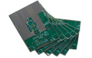
Taconic PCB Design refers to the design of printed circuit boards using Taconic’s specialized high-frequency laminates and dielectric materials for RF, microwave, and high-speed applications.
Taconic materials are available in different formulations designed to provide controlled dielectric constant (Dk), low dissipation factor (Df), thermal stability, dimensional stability, and other characteristics required by high-frequency circuits.
Compared with conventional PCB materials, specialized RF laminates can provide more predictable electrical performance at elevated frequencies. This is particularly important when designing controlled-impedance transmission lines, antennas, filters, amplifiers, RF front ends, and other microwave circuits.
A typical Taconic PCB development process includes:
- Selecting an appropriate Taconic laminate
- Defining the PCB stackup
- Designing transmission lines
- Calculating controlled impedance
- Optimizing grounding and signal return paths
- Completing component placement and routing
- Reviewing manufacturability
- Fabricating and testing the PCB
The exact material and design approach should be selected according to the operating frequency, loss budget, thermal requirements, mechanical constraints, and manufacturing capabilities.
Taconic PCB Transmission-Line Design
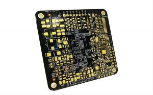
Transmission-line behavior becomes increasingly important as signal frequency rises.
At sufficiently high frequencies, PCB traces can no longer be treated simply as ideal wires. Their electrical behavior depends on distributed parameters such as characteristic impedance, propagation delay, capacitance, inductance, dielectric properties, and conductor geometry.
For this reason, RF and microwave PCB designs commonly use transmission-line models rather than relying exclusively on lumped-circuit assumptions.
The transition between lumped and distributed behavior depends on the electrical length of the interconnect relative to the signal wavelength. Therefore, there is no single universal frequency at which every PCB trace becomes a transmission line.
The designer should evaluate:
- Signal frequency
- Rise and fall time
- Trace length
- Effective dielectric constant
- Electrical wavelength
- Target impedance
- Connector and via discontinuities
This approach provides a more accurate basis for high-frequency PCB Design.
PCB Trace and Frequency Considerations
PCB traces are often relatively short compared with cables or transmission lines used in other systems. However, a short physical trace can still become electrically significant when the signal frequency is high enough.
In high-frequency designs, the effective wavelength inside the PCB dielectric is shorter than the wavelength of the same signal in free space because the propagation velocity is reduced by the dielectric material.
A simplified relationship is:
λg ≈ λ0 / √εeff
where:
- λg is the guided wavelength
- λ0 is the free-space wavelength
- εeff is the effective dielectric constant of the transmission-line structure
This means that both frequency and dielectric properties must be considered when determining whether a PCB interconnect should be treated as a distributed transmission line.
Rather than defining all RF PCBs using one fixed frequency range, engineers should evaluate each signal path according to its actual electrical length and signal characteristics.
Requirements for Taconic Dielectric Substrates
The dielectric substrate is one of the most important elements in an RF or microwave PCB.
For microstrip and other controlled-impedance structures, the substrate should provide stable and predictable electrical characteristics.
Important requirements may include:
Low Dielectric Loss
A low dissipation factor helps reduce dielectric loss, particularly at higher frequencies.
This can be important for circuits with demanding insertion-loss requirements, such as filters, RF amplifiers, antennas, and communication modules.
Stable Dielectric Constant
The dielectric constant should remain sufficiently stable over the required frequency and temperature range.
Changes in Dk can affect:
- Characteristic impedance
- Propagation delay
- Electrical length
- Phase response
- Antenna performance
Thermal Stability
RF and microwave circuits can generate significant heat, particularly when power amplifiers or other high-power components are involved.
The laminate should therefore provide appropriate thermal stability for the intended application.
Dimensional Stability
Dimensional changes can affect layer registration, transmission-line geometry, and impedance.
A stable material helps maintain consistent circuit dimensions during lamination, thermal cycling, and operation.
Surface Quality
The surface should provide appropriate copper adhesion and a consistent structure for fabricating fine RF transmission lines.
Copper Compatibility
The dielectric and copper system must provide reliable adhesion and suitable electrical performance throughout the expected operating environment.
Taconic PCB Thickness
PCB thickness generally refers to the finished board thickness, including the dielectric layers and copper.
Common PCB thicknesses may include approximately:
- 0.8 mm
- 1.0 mm
- 1.2 mm
- 1.6 mm
- 2.0 mm
However, Taconic PCB thickness should not simply be selected according to a standard increment.
For controlled-impedance RF designs, dielectric thickness is an important electrical parameter. Trace width, copper thickness, dielectric thickness, Dk, and reference-plane spacing must be considered together.
For example, changing the dielectric thickness between a microstrip and its reference plane can change the characteristic impedance even when the trace width remains unchanged.
Therefore, the final board thickness and layer structure should be determined during stackup engineering rather than selected independently.
Taconic PCB Copper Thickness
Copper thickness affects both electrical and manufacturing performance.
In RF applications, copper geometry influences conductor resistance, current distribution, thermal performance, and characteristic impedance.
The finished copper thickness should therefore be clearly specified in the fabrication documentation.
Important considerations include:
- Initial copper foil thickness
- Final plated copper thickness
- Copper surface roughness
- Etching tolerance
- Current-carrying requirements
- High-frequency conductor loss
At high frequencies, copper surface roughness can become particularly important because of the skin effect. Excessive roughness can increase the effective path length of high-frequency current and contribute to additional conductor loss.
Taconic PCB Impedance Control
Impedance Control is one of the most critical aspects of Taconic PCB manufacturing.
In RF and microwave systems, 50 Ω transmission lines are common, although other impedance values may be used depending on the circuit architecture.
Characteristic impedance depends on multiple factors, including:
- Dielectric constant
- Dielectric thickness
- Trace width
- Copper thickness
- Transmission-line structure
- Reference-plane configuration
- Copper geometry
For a multilayer PCB, the final dielectric thickness after lamination must also be considered.
Resin Content and Dielectric Thickness
For multilayer structures using prepreg, resin content influences the final dielectric thickness and can affect the effective dielectric properties after lamination.
The actual electrical behavior of a multilayer stackup therefore depends not only on the nominal material specification but also on the manufacturing process.
Lamination pressure, temperature, resin flow, copper pattern density, and material construction can influence the final dielectric geometry.
For demanding RF designs, the PCB material supplier and PCB manufacturer should work together to ensure that the selected material construction is compatible with the required impedance and manufacturing process.
Controlled-Impedance Verification
A professional PCB Manufacturing process may include impedance coupons or other appropriate verification structures.
Depending on the design requirements, impedance can be verified using electrical measurement techniques such as TDR.
This provides a way to confirm that critical transmission lines remain within the specified impedance tolerance.
Taconic PCB Routing Design
Routing is another critical aspect of high-frequency PCB Design.
Unlike low-frequency digital circuits, RF routing requires careful consideration of electromagnetic coupling, return-current paths, transmission-line geometry, and grounding.
Separate Sensitive Analog and Digital Sections
RF, analog, and high-speed digital circuits can interfere with each other if they are poorly arranged.
Sensitive RF transmission lines should therefore be routed away from noisy digital clocks, switching power supplies, and other high-current or high-edge-rate signals whenever practical.
The goal is not simply to increase physical distance, but to control coupling through careful floorplanning, reference planes, routing direction, and return-current paths.
Grounding Design
A continuous and low-inductance reference plane is essential for many RF transmission-line structures.
Designers should avoid unnecessary gaps or discontinuities beneath controlled-impedance traces.
Ground vias can be strategically placed near RF transmission lines, connectors, and circuit boundaries to provide an effective return path.
Via fences may also be used where additional RF isolation is required.
Power Distribution
High-power RF sections require careful power and thermal planning.
High-current power paths should be designed with sufficient copper cross-section and appropriate thermal management.
However, simply adding more copper does not automatically improve RF performance. Copper distribution must be coordinated with impedance requirements, return paths, thermal design, and manufacturability.
Taconic PCB Routing Sequence
A practical RF board layout process can be organized around signal sensitivity and system architecture rather than following one universal routing order.
A typical priority may include:
- RF and microwave transmission lines
- Critical RF-to-baseband interfaces
- Clock and timing signals
- Power distribution
- Digital baseband signals
- Ground and supporting structures
The exact order depends on the system architecture.
Critical RF traces should generally be routed first because their geometry and reference-plane relationship can impose strict layout constraints.
Microstrip and Stripline Structures
Microstrip is one of the most widely used transmission-line structures in RF PCB design.
Common transmission-line structures include:
Surface Microstrip
A surface microstrip consists of a signal trace on the outer layer with a reference plane beneath it, separated by a dielectric layer.
It is relatively easy to manufacture and can provide convenient access for RF components and connectors.
Embedded Microstrip
An embedded microstrip is located within the dielectric structure while remaining associated with a nearby reference plane.
It can provide additional shielding and a different electromagnetic environment compared with an outer-layer microstrip.
Stripline
A stripline is routed between two reference planes.
Because the signal is enclosed between reference planes, stripline can provide strong electromagnetic containment and predictable transmission-line behavior.
Dual Stripline
Dual-stripline configurations use multiple signal layers within a controlled multilayer environment and can be useful for complex high-density RF architectures.
The appropriate transmission-line structure depends on the required impedance, frequency, layer stackup, isolation, manufacturing capability, and mechanical constraints.
Taconic PCB ESD Protection
RF components can be highly sensitive to electrostatic discharge (ESD), particularly certain semiconductor devices and RF integrated circuits.
The ESD sensitivity of a component depends on its construction and manufacturer’s specifications, so designers should not assume one universal ESD threshold for all RF components.
Nevertheless, appropriate ESD protection should be incorporated throughout:
- Component handling
- PCB assembly
- Storage
- Transportation
- Debugging
- Testing
- Rework
Why RF Components Can Be ESD Sensitive
RF components can use specialized semiconductor structures and small geometries that may make them vulnerable to electrical overstress.
Depending on the component technology, damage can result from:
- Electrostatic discharge
- Electrical overstress
- Voltage transients
- Excessive current
- Mechanical stress
- Thermal stress
RF power amplifiers and other high-power devices can also be sensitive to thermal conditions.
Therefore, both electrical protection and thermal management should be considered during design and manufacturing.
ESD Handling Requirements for RF PCBs
A suitable ESD control program should cover the entire manufacturing and assembly environment.
Placement of ESD-Sensitive Components
ESD-sensitive RF components and their associated circuits should be placed according to the assembly and mechanical requirements of the product.
Components that connect directly to external interfaces may require additional protection because external connectors can provide a path for electrostatic discharge.
Identify ESD-Sensitive Components
RF components with strict ESD sensitivity requirements should be clearly identified in production documentation.
This helps manufacturing and assembly personnel apply the appropriate handling procedures.
Use Suitable SMD Components
Surface-mount components are commonly used in RF circuits because they provide compact geometry and can reduce parasitic effects when appropriately selected.
However, the choice between SMD and through-hole components should ultimately be based on the electrical, mechanical, thermal, and assembly requirements of the application.
RF Connector Placement
RF connector placement requires careful consideration.
Signal contacts should be positioned according to the connector manufacturer’s mechanical and electrical requirements. The connector transition from the external interface to the PCB transmission line should also be optimized to minimize impedance discontinuity.
Ground contacts should provide a low-inductance return path and should be connected appropriately to the PCB ground structure.
Taconic PCB Manufacturing Considerations
The performance of a Taconic PCB depends not only on the material itself but also on the manufacturing process.
Important PCB Manufacturing considerations include:
Material Handling
RF laminates should be stored and handled according to the material supplier’s specifications.
Moisture, contamination, mechanical damage, and improper storage can affect material performance and manufacturing yield.
Lamination Control
For multilayer Taconic PCBs, lamination conditions must be carefully controlled.
The final dielectric thickness and layer registration can influence controlled impedance and RF performance.
Drilling
Drilling parameters should be compatible with the selected laminate system.
Poor hole quality, excessive mechanical stress, or dimensional variation can affect vias and plated structures.
Plating
Copper plating should provide consistent thickness and reliable electrical connections.
For RF circuits, via geometry and plating quality can influence parasitic inductance and high-frequency performance.
Etching Accuracy
Because RF impedance is highly dependent on trace geometry, excessive variation in trace width can affect electrical performance.
Precision imaging and etching are therefore important for demanding RF boards.
Electrical Testing
Depending on the application, testing may include:
- Electrical continuity testing
- Insulation resistance testing
- Controlled-impedance testing
- TDR measurement
- Dimensional inspection
- Visual inspection
- RF performance verification
The exact test plan should be established according to the product’s electrical requirements.
Common Taconic PCB Design Mistakes to Avoid
Several design issues can negatively affect RF PCB performance.
Inconsistent Dielectric Thickness
Unexpected variation in dielectric thickness can alter characteristic impedance.
Poor Reference-Plane Design
Gaps or discontinuities beneath RF transmission lines can disrupt return-current paths and increase electromagnetic radiation.
Excessive Via Transitions
Every via transition introduces parasitic inductance and capacitance. Unnecessary transitions should therefore be minimized.
Poor Connector Launch Design
An RF connector cannot be treated as an isolated mechanical component. The connector, PCB pad geometry, vias, transmission line, and reference planes form one electrical transition.
Mixing Noisy Digital and Sensitive RF Routing
High-speed digital clocks and switching power signals can couple into sensitive RF circuits.
Careful floorplanning and routing are therefore essential.
Ignoring Copper Roughness
At higher frequencies, copper roughness can contribute to conductor loss and should be included in the RF loss budget where appropriate.
Taconic PCB Applications
Taconic-based PCB technologies can be used in a wide range of high-frequency applications.
Telecommunications
Applications include:
- RF communication modules
- Wireless infrastructure
- Base stations
- Microwave links
- Satellite communication
- High-frequency networking equipment
Aerospace and Defense
High-frequency laminates can be used in:
- Radar systems
- Avionics
- Satellite electronics
- RF communication systems
- Navigation equipment
- Electronic sensing systems
Automotive Electronics
Automotive RF applications include:
- Radar sensors
- ADAS systems
- Wireless communication modules
- Vehicle connectivity
- High-frequency sensing equipment
Medical Electronics
RF and microwave PCB technologies can also support specialized medical and diagnostic equipment where stable high-frequency electrical performance is required.
Industrial and Test Equipment
Specialized RF laminates are used in measurement systems, test equipment, signal generators, filters, antennas, and other high-frequency electronic products.
Conclusion
Taconic PCB technology provides a specialized foundation for high-frequency, RF, microwave, and high-speed electronic applications. Its value comes from the electrical, thermal, and mechanical characteristics of the selected laminate rather than from the material name alone.
A successful Taconic PCB requires close coordination between material selection, stackup engineering, transmission-line design, impedance control, grounding, routing, ESD handling, and manufacturing.
During PCB Design, engineers should carefully evaluate Dk, Df, dielectric thickness, copper thickness, transmission-line geometry, return paths, connector transitions, and thermal requirements.
During PCB Manufacturing, the manufacturer must maintain appropriate control over lamination, dielectric thickness, copper geometry, drilling, plating, etching, registration, and impedance verification.
When material selection and manufacturing processes are properly matched to the electrical requirements, Taconic-based PCB technology can provide stable and predictable performance for demanding RF and microwave systems.
Article Summary
Taconic PCB technology is commonly used for high-frequency and RF applications that require controlled dielectric properties, low loss, stable dimensions, and reliable signal integrity.
The most important aspects of Taconic PCB Design include material selection, transmission-line configuration, impedance control, grounding, RF routing, copper geometry, and connector transitions. Microstrip, embedded microstrip, and stripline are among the transmission-line structures that can be used depending on the stackup and application.
For PCB Manufacturing, dielectric thickness, resin construction, copper thickness, surface roughness, lamination, drilling, plating, and etching accuracy can all affect final RF performance. Controlled-impedance testing may also be required for demanding designs.
Taconic PCB materials are therefore best treated as part of an integrated RF design and manufacturing system. The laminate, PCB geometry, component selection, layout, fabrication process, and testing strategy must work together to achieve reliable high-frequency performance.