Inverter PCB Design: PCB Design, PCB Manufacturing & High-Power Layout Guide
Inverter technology plays a critical role in modern electronic and power-conversion systems. By converting direct current (DC) into alternating current (AC), inverters enable efficient power conversion and control across applications such as renewable energy systems, electric vehicles, industrial equipment, energy storage systems, motor drives, and consumer electronics.
The PCB Design of an inverter is particularly important because the circuit board must handle high currents, switching transients, thermal loads, electromagnetic interference (EMI), and potentially high voltages within a relatively compact space.
Unlike conventional low-power circuit boards, inverter PCBs require careful consideration of current paths, copper thickness, component placement, grounding, thermal management, creepage and clearance, and power-loop area.
This guide explains the fundamentals of inverter PCB design, five important design steps, and key inverter PCB layout principles for reliable power electronics.
What Is Inverter PCB Design?
Inverter PCB design is the process of designing a printed circuit board that supports the conversion of DC power into AC power.
A typical inverter circuit may include:
- Power semiconductor devices
- MOSFETs or IGBTs
- Gate-driver circuits
- DC-link capacitors
- Inductors
- Transformers
- Microcontrollers or processors
- Current and voltage sensors
- Protection circuits
- Filtering components
- Communication interfaces
The PCB must provide reliable electrical connections between these components while managing current, voltage, heat, switching noise, and electromagnetic interference.
For this reason, inverter PCB Design requires more than simply placing components and routing electrical connections. The designer must understand power electronics, PCB materials, thermal behavior, signal integrity, EMC, and manufacturing constraints.
5 Key Steps in Inverter PCB Design
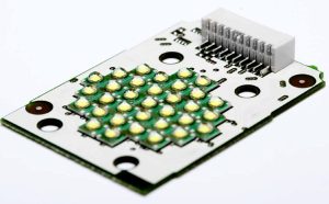
Designing an inverter PCB can be challenging, especially for high-power applications. The following five steps can help engineers establish a reliable and manufacturable design.
1. PCB Layout
PCB layout should be considered from the earliest stage of inverter development.
One of the most important principles in inverter PCB layout is to understand and control the current paths. The magnitude and location of current directly influence PCB heating, voltage drop, electromagnetic interference, and overall power loss.
Important factors include:
- Power level
- Maximum operating current
- Operating temperature
- Airflow and cooling conditions
- PCB material
- Copper thickness
- Component density
- Switching frequency
- Power-loop area
Trace Layout
For high-current inverter circuits, trace resistance must be minimized.
As trace length increases, resistance and parasitic inductance generally increase. Higher resistance results in greater I²R power loss and heat generation.
Therefore, high-current paths should generally be:
- As short as practical
- As wide as practical
- Properly connected to copper planes
- Designed with controlled current-return paths
For high-current applications, engineers can use IPC design guidance and validated PCB trace-width calculations to determine an appropriate conductor width based on current, copper thickness, temperature rise, and other design parameters.
The actual trace width should not be selected based on current alone. Temperature rise, copper thickness, internal versus external layer location, allowable voltage drop, and manufacturing capability should also be considered.
Copper Thickness
Copper thickness is another important consideration in high-power inverter PCB design.
Standard PCBs often use copper thicknesses such as 17.5 μm (0.5 oz) or 35 μm (1 oz). High-current inverter applications may require thicker copper, such as:
- 35 μm — 1 oz
- 70 μm — 2 oz
- 105 μm — 3 oz
- Higher copper weights for specialized heavy-copper applications
Increasing copper thickness can reduce conductor resistance and improve current-carrying capability. It can also allow designers to achieve the required current capacity without making traces excessively wide.
However, thicker copper affects PCB Manufacturing requirements and may increase fabrication cost. It can also influence etching, plating, minimum feature size, via design, soldering, and thermal behavior.
Therefore, copper thickness should be selected according to the electrical requirements and the manufacturer’s manufacturing capabilities.
2. Component Placement
Component placement is particularly important in inverter PCB design because power devices can generate substantial heat.
Power components such as MOSFETs, IGBTs, rectifiers, voltage regulators, and power converters should be positioned according to current paths and thermal requirements.
Place High-Power Components Carefully
High-power components should not be positioned randomly or packed into a small area.
Concentrating multiple high-power devices in one location can create a thermal hotspot and increase the local PCB temperature.
The designer should consider:
- Heat generation
- Heat dissipation
- Airflow
- Heat-sink location
- Thermal vias
- Copper planes
- Distance from temperature-sensitive components
High-density digital components such as microcontrollers, processors, and FPGAs should also be separated appropriately from high-power switching circuits.
Minimize High-Current Loops
High-current loops should be kept as small as practical.
Large current loops increase parasitic inductance and can produce stronger electromagnetic radiation during fast switching.
A well-designed inverter PCB should therefore minimize the loop area formed by:
- Power switches
- DC-link capacitors
- Gate drivers
- Output devices
- Return paths
The DC-link capacitor should generally be placed close to the switching devices to minimize the high-frequency power loop.
Separate Power and Sensitive Circuits
Power switching circuits and sensitive control circuits should be physically separated where practical.
Sensitive circuits may include:
- Analog sensing circuits
- Current-sensing circuits
- Voltage feedback circuits
- Microcontrollers
- Communication interfaces
- Gate-control signals
Separating these circuits can help reduce coupling from high-current and high-frequency switching paths.
Establish a Controlled Grounding Strategy
Grounding is critical in inverter PCB design.
Engineers should define the current-return paths rather than allowing return currents to flow through unintended areas of the PCB.
Depending on the system architecture, designers may use:
- Power ground
- Signal ground
- Analog ground
- Chassis ground
- Protective earth
The exact grounding strategy depends on the inverter topology, isolation requirements, switching frequency, and system safety architecture.
3. Thermal Management
Thermal management is one of the most important considerations in high-power inverter PCB design.
Power semiconductors, regulators, resistors, inductors, and other components generate heat during operation. If this heat cannot be removed effectively, component temperatures can rise beyond their specified operating limits.
Excessive temperature can reduce component reliability and accelerate aging.
Increase Copper Area
Increasing copper area is one of the simplest ways to improve heat spreading.
Large copper planes can distribute heat away from high-power components and increase the effective heat-spreading area.
Copper planes can also reduce electrical resistance and voltage drop in high-current paths.
Use Thermal Vias
Thermal vias can transfer heat from a component’s PCB pad or copper region into internal or opposite-side copper layers.
An array of thermal vias can help distribute heat through the PCB and improve thermal performance when appropriately designed.
Thermal-via design should consider:
- Via diameter
- Via pitch
- Via quantity
- Plating quality
- Pad geometry
- Manufacturing capability
- Solder wicking concerns
Keep Temperature-Sensitive Components Away From Heat Sources
Some components are particularly sensitive to temperature changes.
Examples include:
- Voltage references
- Precision amplifiers
- Current-sensing circuits
- Temperature sensors
- Oscillators
- Certain regulators
- Analog measurement circuits
These components should be positioned away from high-temperature power devices when possible.
Thermal isolation can help reduce measurement errors and improve long-term system stability.
4. Removing Solder Mask for High-Current Applications
Another technique sometimes used in high-current PCB design is selectively removing solder mask from specific copper areas.
Exposing the copper surface can allow additional solder or copper reinforcement to be applied to increase the effective conductor thickness.
This approach may be used when designers need higher current-carrying capability without significantly increasing the PCB trace width.
However, exposed copper introduces additional manufacturing, assembly, oxidation, contamination, and safety considerations.
Therefore, solder-mask removal should be treated as a specialized design technique rather than a universal solution.
The designer should confirm the process with the PCB manufacturer before incorporating it into production.
5. Decoupling Capacitors
Decoupling capacitors are essential components in many inverter PCB designs.
Fast switching devices can produce transient currents and voltage fluctuations. If the power distribution network has excessive impedance, these transient currents can cause voltage dips, ringing, and electromagnetic interference.
A properly positioned decoupling capacitor provides a local source of transient current and reduces the effective impedance between the power rail and ground.
Proper Decoupling Capacitor Placement
The capacitor should generally be placed as close as practical to the power pins of the device it supports.
The connection path between the capacitor and the device should be:
- Short
- Wide where appropriate
- Low impedance
- Properly referenced to the intended ground plane
The capacitor’s return connection should also be short and direct.
Choosing a Decoupling Capacitor
Capacitor selection depends on:
- Required capacitance
- Operating voltage
- Equivalent series resistance (ESR)
- Equivalent series inductance (ESL)
- Dielectric material
- Package size
- Switching frequency
- Temperature
- DC-bias characteristics
Ceramic capacitors are frequently used for high-frequency decoupling because of their low ESR and ESL.
However, a single capacitor value should not be treated as universally applicable. The required capacitance and capacitor combination should be determined from the power-distribution network and transient-current requirements of the specific inverter.
Inverter PCB Layout Principles
As electronic systems become smaller and power density increases, inverter PCB layout requires careful control of electrical, thermal, and electromagnetic behavior.
The following principles can help engineers develop a more robust inverter PCB.
Critical Signal Priority
Critical signals should receive priority during PCB layout.
These may include:
- High-speed signals
- Clock signals
- Synchronization signals
- Gate-drive signals
- Current-sensing signals
- Voltage-feedback signals
- Communication interfaces
Critical signals should be routed according to their electrical requirements rather than simply following the shortest available path.
Density-First Placement
For complex PCBs, placement should begin with components that have the most important electrical or mechanical relationships.
High-density functional blocks should be positioned first, followed by less critical components.
This approach can help optimize:
- Routing space
- Power distribution
- Signal integrity
- Thermal management
- Component accessibility
Minimize Current-Loop Area
One of the fundamental principles of power PCB layout is minimizing current-loop area.
When a signal or power current flows through a circuit, it must return through an appropriate path.
If the outgoing and return paths are separated by a large distance, the resulting loop area increases.
A larger loop can increase electromagnetic radiation and susceptibility to external interference.
Keeping the forward and return paths close together can reduce loop inductance and improve EMC performance.
Avoid Unintended Open-Ended Traces
Unconnected or improperly terminated traces can behave like antennas, particularly at high frequencies.
Unnecessary stubs and floating copper structures should therefore be minimized.
High-frequency signals should be routed with appropriate termination and impedance-control strategies.
Impedance Matching
Impedance control is important for high-speed and high-frequency inverter control circuits.
Changes in trace width, dielectric thickness, reference-plane geometry, and routing structure can change characteristic impedance.
Therefore, controlled-impedance traces should maintain consistent geometry along the signal path whenever possible.
For high-speed interfaces, impedance requirements should be defined during the PCB Design stage and verified during PCB Manufacturing using appropriate fabrication controls and testing methods.
Maintain Power and Ground Plane Integrity
Power and ground planes should be designed carefully to maintain low-impedance current-return paths.
Dense via fields can create unexpected interruptions or narrow sections in power and ground planes.
Designers should therefore examine whether vias, cutouts, mounting holes, and other PCB features unintentionally divide a reference plane.
Maintaining a continuous reference plane can help reduce return-path discontinuities and unwanted electromagnetic coupling.
Avoid Unnecessary Power-Plane Overlap
Different power domains should be arranged carefully to minimize unwanted coupling.
Particular attention should be paid to areas where power regions with significantly different voltage levels are positioned close to one another.
Where separation is necessary, an appropriate ground or shielding structure may be used between power regions.
The final strategy should be determined according to the inverter topology, voltage levels, switching frequency, isolation requirements, and EMC targets.
Important Manufacturing Considerations for Inverter PCBs
A technically sound inverter PCB design must also be manufacturable.
During PCB Manufacturing, engineers and manufacturers should consider:
- Copper thickness
- Minimum trace width
- Minimum spacing
- Via dimensions
- Hole aspect ratio
- PCB thickness
- Surface finish
- Solder mask
- Thermal-via fabrication
- Heavy-copper requirements
- Layer stackup
- Creepage and clearance
- Assembly process
- Testing requirements
High-power inverter boards may require heavy copper or specialized PCB structures. These requirements should be discussed with the PCB manufacturer before the design is finalized.
DFM analysis can identify manufacturing problems early and help avoid expensive redesigns.
Inverter PCB Design: Electrical and Safety Considerations
High-voltage inverter PCBs require additional attention to electrical safety.
Designers should evaluate:
- Creepage distance
- Clearance distance
- Isolation requirements
- Working voltage
- Transient voltage
- Insulation system
- PCB material
- Contamination level
- Environmental conditions
- Applicable safety standards
Creepage refers to the shortest distance along the surface of an insulating material between conductive parts, while clearance refers to the shortest distance through air.
These requirements should be established according to the applicable product safety standards and system voltage.
For high-voltage inverter applications, spacing should never be selected solely according to general low-voltage PCB rules.
Common Applications of Inverter PCBs
Inverter PCB technology is widely used in modern power electronics.
Typical applications include:
Solar Inverters
Solar inverters convert DC power generated by photovoltaic panels into AC power suitable for electrical loads or grid connection.
Energy Storage Systems
Battery energy storage systems use bidirectional power converters and inverter circuits to control energy flow between batteries and AC systems.
Electric Vehicles
Inverters are essential components in electric vehicle powertrains, where they control the conversion of battery DC power into AC power for electric motors.
Motor Drives
Industrial motor drives use inverter circuits to control motor speed, torque, and operating efficiency.
Uninterruptible Power Supplies
UPS systems use inverter circuits to provide AC power when the primary electrical supply is unavailable.
How Kingda Can Support Inverter PCB Projects
Inverter applications often require close coordination between PCB design, fabrication, assembly, and testing.
Kingda can support electronic manufacturing projects involving:
- PCB Design
- PCB Manufacturing
- High-current PCB fabrication
- Multilayer PCB manufacturing
- Heavy-copper PCB manufacturing
- SMT assembly
- PTH assembly
- Component sourcing
- PCB testing
- Functional testing
- DFM analysis
- Quality inspection
For high-power inverter projects, design and manufacturing requirements should be discussed early so that electrical, thermal, mechanical, and manufacturing constraints can be incorporated into the PCB development process.
Summary
Inverter PCB design is a specialized area of PCB Design that requires careful consideration of current capacity, copper thickness, component placement, thermal management, decoupling, grounding, electromagnetic interference, impedance control, and electrical safety.
For high-power applications, PCB traces and power loops should be designed to minimize resistance, parasitic inductance, voltage drop, and heat generation. High-power components should be positioned according to both electrical and thermal requirements, while sensitive control circuits should be protected from switching noise and excessive heat.
At the same time, a successful design must be compatible with PCB Manufacturing processes. Copper thickness, via structures, spacing, thermal vias, PCB materials, surface finish, and assembly requirements should all be considered before production.
By combining sound electrical design principles with appropriate thermal management, EMC control, DFM practices, and manufacturing expertise, engineers can develop inverter PCBs that provide stable performance and reliable operation in demanding power-electronics applications.