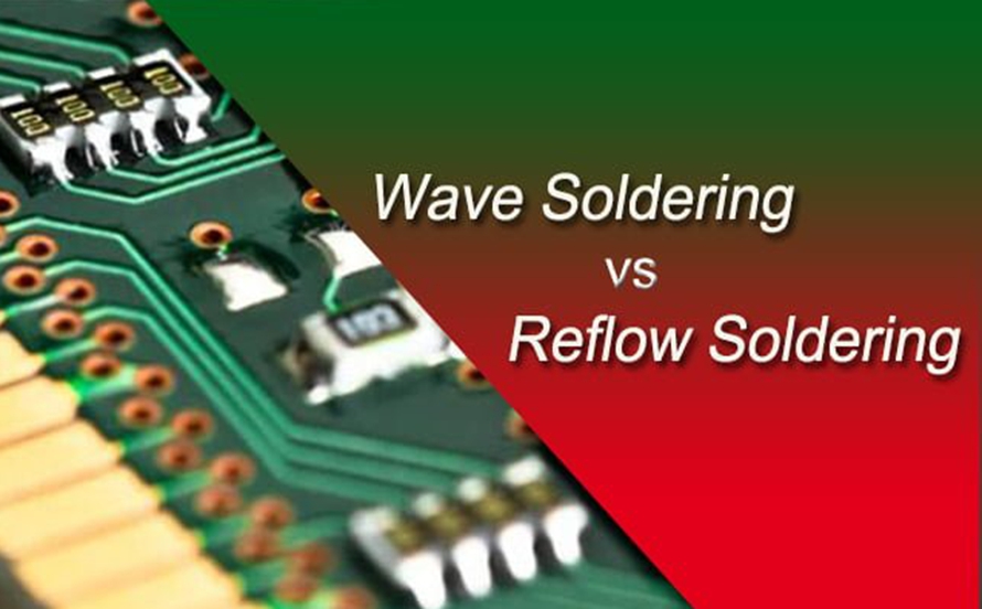
Reflow Soldering vs Wave Soldering: PCB Design, PCB Manufacturing & PCBA Guide
Reflow soldering and wave soldering are two fundamentally different technologies used in PCB Assembly and electronic manufacturing. Both processes are widely used in the electronics industry, and a single PCB assembly may require both methods depending on the types of components and solder joints involved.
Although both technologies create reliable solder joints between electronic components and a PCB, they differ significantly in their applications, equipment, soldering processes, component compatibility, thermal profiles, and production requirements.
Reflow soldering is primarily associated with surface-mount technology (SMT), while wave soldering is traditionally used for through-hole technology (THT) components. However, modern PCB assemblies often combine SMT and THT components, making it important for manufacturers to understand when and how each soldering process should be used.
This article explains the major differences between Reflow Soldering and Wave Soldering, including their equipment, processes, components, solder materials, advantages, limitations, and applications in modern PCB Manufacturing.
What Are Reflow Soldering and Wave Soldering?
What Is Reflow Soldering?
Reflow soldering is a thermal soldering process primarily used for SMT PCB Assembly.
During the process, solder paste is first deposited onto the PCB pads using a stencil printer. SMT components are then accurately placed onto the solder paste. The populated PCB passes through a reflow oven where it is gradually heated according to a controlled temperature profile.
As the temperature increases, the solder paste melts and forms reliable solder joints between the component terminals and PCB pads. The assembly is subsequently cooled under controlled conditions.
A typical reflow soldering process includes:
- Solder paste printing
- Solder paste inspection (SPI)
- SMT component placement
- Reflow soldering
- Automated optical inspection (AOI)
- X-ray inspection when required
- Electrical and functional testing
Because the process can accurately solder a large number of small components simultaneously, reflow soldering is widely used for high-density and complex PCB assemblies.
What Is Wave Soldering?
Wave soldering is a mass soldering process primarily used for Through-Hole PCB Assembly.
Instead of placing solder paste on individual pads and heating the entire PCB through a reflow profile, wave soldering uses a bath of molten solder. A pump creates a controlled wave of molten solder, and the PCB passes over the wave so that exposed solderable surfaces, particularly through-hole component leads, contact the molten solder.
A typical wave soldering process includes:
- PCB preparation
- Through-hole component insertion
- Flux application
- Preheating
- Contact with the molten solder wave
- Cooling
- Inspection and testing
Wave soldering is particularly useful for boards containing large numbers of through-hole components or components that require strong mechanical solder joints.
Reflow Soldering vs Wave Soldering: Key Differences
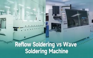
Reflow soldering and wave soldering can both produce high-quality solder joints, but their operating principles are very different.
| Feature | Reflow Soldering | Wave Soldering |
|---|---|---|
| Primary application | SMT assembly | THT/through-hole assembly |
| Solder delivery | Solder paste applied to pads | Molten solder wave |
| Main equipment | Reflow oven | Wave soldering machine |
| Component placement | Components placed before heating | Through-hole leads pass through solder wave |
| PCB side | Usually suitable for surface-mounted components | Primarily used for one solder side at a time |
| Thermal process | Controlled multi-zone heating profile | Preheat + molten solder contact |
| Typical applications | High-density PCB assemblies | Through-hole and mixed-technology boards |
| Production suitability | Excellent for high-density SMT | Effective for high-volume THT soldering |
| Solder material | Solder paste | Molten solder alloy |
| Inspection | SPI, AOI, X-ray, electrical testing | Visual inspection, AOI, electrical testing |
Different Equipment and Processes
One of the most obvious differences between reflow soldering and wave soldering is the equipment used.
Reflow Soldering Equipment
The primary equipment is a reflow oven.
A modern reflow oven generally contains multiple independently controlled heating and cooling zones. The PCB travels through these zones on a conveyor while the temperature is carefully controlled.
A typical thermal profile includes:
- Preheat
- Thermal soak
- Reflow
- Cooling
During the reflow stage, the solder alloy reaches a temperature above its melting point. The exact temperature and time depend on the solder alloy, PCB design, component requirements, and manufacturer’s process specifications.
The purpose of the thermal profile is not simply to melt the solder. It must also control heating rates, time above liquidus, peak temperature, and cooling rate to achieve reliable solder joints while minimizing thermal stress.
Wave Soldering Equipment
Wave soldering machines use a different operating principle.
A typical machine contains:
- Fluxing system
- Preheating section
- Molten solder pot
- Solder pump
- Wave nozzle
- Conveyor
- Cooling section
- Process monitoring system
The solder is maintained in a molten state inside the solder pot. A pump generates a controlled wave of solder, and the PCB passes over it at a defined speed and angle.
The molten solder contacts the exposed through-hole leads and corresponding PCB pads, forming solder joints.
Modern wave soldering machines may use different wave configurations, including turbulent and laminar waves, depending on the PCB design and component requirements.
Different Soldering Processes
The basic process flows of the two technologies are also different.
Typical Reflow Soldering Process
Solder Paste Printing → SPI → SMT Component Placement → Reflow Oven → AOI → X-Ray if Required → Electrical Testing → Functional Testing
The process begins by printing solder paste onto the PCB pads through a stencil.
The SMT placement machine then positions components accurately onto the printed solder paste.
The populated board enters the reflow oven, where the solder paste passes through a controlled thermal profile and forms solder joints.
AOI is commonly used after reflow to detect defects such as:
- Missing components
- Misaligned components
- Incorrect component orientation
- Solder bridges
- Insufficient solder
- Excessive solder
- Tombstoning
X-ray inspection may be used for hidden solder joints, such as certain bottom-terminated components and area-array packages.
Typical Wave Soldering Process
THT Component Insertion → Flux Application → Preheating → Wave Soldering → Cooling → Inspection → Electrical Testing
Through-hole components are inserted into the PCB before the board enters the wave soldering machine.
Flux is applied to improve solderability and promote proper wetting. The PCB is then preheated before passing over the molten solder wave.
As the solder wave contacts the underside of the PCB, molten solder fills the plated through-holes and forms solder joints around the component leads.
After soldering, the PCB is cooled and inspected.
Different Types of Components
Component compatibility is another major difference between the two processes.
Reflow Soldering for SMT Components
Reflow soldering is primarily designed for surface-mount components.
Examples include:
- Resistors
- Capacitors
- Diodes
- LEDs
- Transistors
- SOIC packages
- QFP packages
- QFN packages
- BGA packages
- LGA packages
- Other SMT packages
Because SMT components can be extremely small and densely positioned, reflow soldering is particularly suitable for compact electronic products.
Wave Soldering for Through-Hole Components
Wave soldering is mainly used for through-hole components whose leads extend through PCB holes.
Common examples include:
- Large connectors
- Terminal blocks
- Transformers
- Relays
- Switches
- Large capacitors
- Power components
- Certain mechanically stressed components
Through-hole components can provide strong mechanical connections because their leads pass through the PCB.
Mixed-Technology PCB Assembly
Modern PCBs frequently contain both SMT and through-hole components.
For this reason, a PCB assembly may require both reflow and wave soldering.
A typical mixed-technology production sequence may be:
SMT Solder Paste Printing → SMT Placement → Reflow Soldering → THT Component Insertion → Wave Soldering → Inspection → Testing
In some applications, selective soldering is used instead of conventional wave soldering.
Selective soldering uses a controlled localized solder fountain to solder specific through-hole joints without exposing the entire PCB underside to a conventional solder wave.
This can be especially useful when a board contains sensitive SMT components on the same side or when only a limited number of through-hole joints need soldering.
Different Solder Materials
The solder material and delivery method also differ.
Solder Paste for Reflow Soldering
Reflow soldering generally uses solder paste.
Solder paste consists primarily of fine solder alloy particles mixed with flux and other materials that provide the required printing and handling characteristics.
Common lead-free solder alloys include SAC-family alloys containing tin, silver, and copper.
The solder paste is deposited onto PCB pads using a stencil and then melted during the reflow process.
The paste formulation must be compatible with:
- PCB surface finish
- Component requirements
- Reflow temperature
- Stencil printing process
- Production environment
Molten Solder for Wave Soldering
Wave soldering uses molten solder contained in a solder pot.
Common lead-free wave solder alloys are also based on tin with appropriate alloying elements, while legacy processes may use tin-lead alloys where permitted.
The solid solder is melted inside the machine and maintained at a controlled temperature. A pump then generates the solder wave that contacts the PCB.
Unlike reflow soldering, solder is not applied to individual pads as a printed paste layer immediately before component placement.
Thermal Profile Differences
Thermal control is critical in both processes, but the thermal environment is different.
Reflow Thermal Profile
Reflow soldering typically uses a controlled multi-stage profile:
Preheat → Soak → Reflow → Cooling
The profile must be optimized according to the solder paste manufacturer’s specifications and the thermal limitations of the components and PCB.
Important parameters include:
- Ramp rate
- Soak time
- Peak temperature
- Time above liquidus
- Cooling rate
Incorrect thermal settings can result in solder defects, component damage, poor wetting, or excessive intermetallic growth.
Wave Soldering Thermal Process
Wave soldering generally uses:
Fluxing → Preheating → Molten Solder Contact → Cooling
The PCB is exposed to a short period of direct contact with molten solder.
The conveyor speed, preheat temperature, solder temperature, board orientation, flux quantity, and contact conditions must be carefully controlled.
Advantages of Reflow Soldering
Reflow soldering provides several advantages for modern electronics manufacturing.
High Component Density
Reflow soldering is highly suitable for compact SMT layouts with small components and fine-pitch packages.
Excellent Process Repeatability
Automated printing, placement, and thermal profiling allow manufacturers to maintain consistent production conditions.
Suitable for Complex PCBs
High-density multilayer PCBs can contain hundreds or thousands of SMT components, making automated reflow soldering an efficient production solution.
Compatible with Automated Inspection
SPI, AOI, X-ray inspection, and automated testing can be integrated into the SMT production line.
Advantages of Wave Soldering
Wave soldering also provides important benefits.
Efficient Through-Hole Soldering
Large numbers of through-hole joints can be soldered efficiently in a continuous process.
Strong Mechanical Connections
Through-hole components provide mechanical anchoring in addition to electrical connections.
Suitable for Large Components
Some large connectors, power components, transformers, and other mechanically demanding components are well suited to through-hole assembly.
Limitations of Reflow Soldering
Despite its advantages, reflow soldering has some limitations.
- Some large through-hole components cannot be easily processed through standard SMT reflow.
- Certain components may have strict thermal limitations.
- Complex boards may require careful thermal profiling.
- Large thermal-mass components can affect temperature uniformity.
- Defects such as tombstoning and solder bridging can occur if the process is not properly controlled.
Limitations of Wave Soldering
Wave soldering also has limitations.
- It is primarily intended for through-hole solder joints.
- Fine-pitch SMT components are generally not suited to conventional wave soldering.
- PCB orientation and component layout must be carefully considered.
- Shadowing effects can occur when components obstruct the solder wave.
- Excess solder can create bridges or other solder defects.
- Flux management and solder-pot maintenance are important process controls.
Reflow Soldering vs Wave Soldering: Which Should You Use?
The appropriate soldering technology depends on the PCB design, component technology, production volume, thermal requirements, and assembly structure.
Reflow soldering is generally suitable when the PCB contains a high proportion of SMT components and requires compact, high-density assembly.
Wave soldering is generally suitable when the PCB contains many through-hole components that can be efficiently soldered using a molten solder wave.
For mixed-technology PCB assemblies, manufacturers may use a combination of reflow, wave soldering, selective soldering, and manual soldering.
Therefore, the choice should be made during the PCB Design and manufacturing-planning stages rather than after the PCB has already been fabricated.
How PCB Design Affects Soldering
Soldering performance depends heavily on PCB layout.
During PCB Design, engineers should consider:
- Component orientation
- Component spacing
- Pad dimensions
- Land patterns
- Thermal relief
- Copper distribution
- Via placement
- Solder mask design
- Through-hole dimensions
- Component height
- Board orientation
- Assembly access
- Thermal sensitivity
For wave soldering, component orientation is particularly important because the board passes through a solder wave in a defined direction.
Poor placement can create shadowing and prevent molten solder from reaching certain joints.
For reflow soldering, pad geometry and component symmetry are important because they influence solder paste deposition, wetting, and component balance during melting.
PCB Manufacturing and Assembly Quality Control
Reliable PCB Manufacturing requires more than selecting the correct soldering process.
Manufacturers should establish appropriate process controls throughout the production line.
Important quality-control methods include:
- Solder Paste Inspection (SPI)
- Automated Optical Inspection (AOI)
- X-ray inspection
- Visual inspection
- Electrical testing
- In-Circuit Testing (ICT)
- Functional testing
- Reflow profile verification
- Wave soldering parameter monitoring
- Solderability testing when required
These inspection methods help identify defects before the assembled PCB reaches the final product.
Reflow Soldering and Wave Soldering at Kingda
For reliable PCB Assembly and PCB Manufacturing, the soldering process should be selected according to the PCB design and component requirements.
Kingda can support PCB assembly projects involving SMT, THT, and mixed-technology assemblies. Depending on the product structure, the manufacturing process may incorporate reflow soldering, wave soldering, selective soldering, manual assembly, AOI, X-ray inspection, and electrical testing.
During manufacturing preparation, engineers can evaluate component packages, PCB layout, soldering requirements, thermal limitations, and inspection requirements to establish a suitable production process.
A properly coordinated process from PCB Design through PCB Manufacturing and final PCB assembly can improve production consistency and reduce assembly-related defects.
Summary
Reflow soldering and wave soldering are both important technologies in modern PCB Assembly, but they operate according to fundamentally different principles.
Reflow soldering uses printed solder paste and a controlled thermal profile to solder primarily SMT components. It is particularly suitable for compact, high-density, and highly automated PCB assemblies.
Wave soldering uses a controlled wave of molten solder and is primarily intended for through-hole components. It is useful for large components, connectors, and assemblies where mechanical strength and efficient THT soldering are important.
Modern electronic products often combine SMT and THT technologies. As a result, manufacturers may use reflow soldering, wave soldering, selective soldering, or a combination of these processes.
Understanding the differences between these technologies allows engineers and purchasing teams to make better decisions during PCB Design, PCB Manufacturing, and PCBA process planning.