Control PCB: PCB Design, PCB Manufacturing & Industrial Control Board Guide
In modern electronics, a Control PCB serves as the electronic control center that coordinates signals, processes inputs, executes programmed logic, and manages the operation of connected devices. Unlike a conventional PCB that primarily provides electrical interconnections between components, a control board typically integrates processing devices, communication interfaces, input/output circuits, power-management circuits, and other functional blocks.
Control PCBs are widely used in automotive electronics, industrial automation, consumer electronics, medical equipment, telecommunications, robotics, smart devices, and other technology-intensive applications. As products become more connected and intelligent, control boards increasingly require compact layouts, reliable signal transmission, efficient thermal management, robust testing, and advanced PCB Design.
This article explains what a control PCB is, its structure and types, design considerations, manufacturing and assembly processes, applications, advantages, challenges, and future development trends.
What Is a Control PCB?
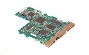
A control PCB is a printed circuit board designed to receive inputs, process information, execute control logic, and generate outputs for a specific electronic system.
A conventional PCB may primarily provide conductive paths and mechanical support for electronic components. A control PCB, by contrast, generally incorporates the circuitry required to make decisions and control other parts of a system.
A typical control PCB may include:
- Microcontrollers (MCUs)
- Microprocessors or system-on-chip devices
- Digital and analog circuits
- Sensors and signal-conditioning circuits
- Input/output interfaces
- Communication interfaces
- Power-management circuits
- Memory devices
- Driver circuits
- Protection components
The controller may receive information from sensors or user interfaces, process that information according to programmed logic, and then send commands to actuators, motors, displays, relays, communication modules, or other electronic subsystems.
Therefore, a control PCB is better understood as a functional electronic control platform rather than simply a physical PCB substrate.
Structure of a Control PCB
The structure of a control PCB depends on its application, layer count, operating environment, electrical requirements, and component density.
A typical control PCB may contain the following elements.
PCB Substrate
FR-4 is widely used for general-purpose control boards because it provides a useful combination of mechanical strength, electrical insulation, processability, and cost.
Other materials may be selected when the application requires special electrical, thermal, mechanical, or environmental characteristics. For example, high-frequency laminates may be used for RF interfaces, while flexible or rigid-flex materials may be selected when the product requires bending or three-dimensional installation.
Copper Layers
Copper layers provide the conductive paths used to transmit power and electrical signals.
Multilayer control boards may contain dedicated signal, power, and ground layers. A properly designed ground and power structure can help improve signal integrity and reduce electromagnetic interference.
Solder Mask
The solder mask covers selected areas of the copper surface and helps prevent accidental solder bridging and environmental contamination.
Although green is the most common solder-mask color, control PCBs can also use other colors depending on the application and manufacturing requirements.
Silkscreen
The silkscreen provides reference designators, polarity indicators, connector labels, test-point markings, and other assembly information.
It acts as a visual guide during PCB assembly, inspection, maintenance, and troubleshooting.
Microcontroller or Processor
The MCU or processor is often the primary control device.
It executes firmware, processes sensor inputs, communicates with other devices, and generates control signals. The specific processor architecture depends on processing requirements, memory requirements, communication interfaces, power consumption, and software requirements.
Input/Output Interfaces
I/O circuits allow the control PCB to communicate with external devices.
Depending on the application, interfaces may include:
- GPIO
- ADC
- DAC
- UART
- SPI
- I²C
- CAN
- USB
- Ethernet
- RS-485
The appropriate interface depends on the system architecture and communication requirements.
Types of Control PCBs
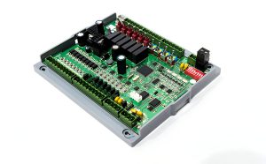
Control PCBs can be classified according to their processing architecture, circuit type, application, and degree of customization.
Programmable Control PCBs
Programmable control boards use a programmable device such as an MCU, MPU, PLC-related processor, or embedded controller.
The behavior of the system can be changed by modifying firmware or software rather than redesigning the entire PCB.
Microcontroller-Based Control PCBs
MCU-based control boards are common in embedded systems.
The microcontroller may integrate a processor core, memory, timers, ADCs, communication interfaces, and other peripherals into a single device.
These boards are widely used in appliances, automotive modules, industrial controllers, sensors, IoT products, and consumer electronics.
Analog Control PCBs
Analog control boards use analog circuits to process continuously varying signals.
Typical circuits may include:
- Operational amplifiers
- Comparators
- Filters
- Voltage references
- Analog signal-conditioning circuits
- ADC interfaces
Analog circuitry is particularly important when the system needs to accurately process signals from sensors or other analog sources.
Digital Control PCBs
Digital control boards process information primarily as digital signals.
They may include:
- Logic gates
- Counters
- Digital processors
- Memory
- Digital communication interfaces
- FPGA or programmable logic devices
Digital control is widely used in modern embedded systems because it supports complex logic, communication, data processing, and firmware-based control.
Custom Control PCBs
Custom control PCBs are developed for specific products or industrial systems.
Instead of relying on a generic controller board, the manufacturer can integrate the processor, interfaces, power circuits, communication functions, sensors, and protection circuits into a customized PCB.
This approach can reduce unnecessary components and optimize the board for the intended product.
Control PCB vs. Power PCB
Control PCBs and power PCBs can work together within the same electronic system, but their primary functions are different.
| Feature | Control PCB | Power PCB |
|---|---|---|
| Primary function | Signal processing, control logic, communication, and system management | Power conversion, switching, distribution, and regulation |
| Typical components | MCU, processor, sensors, communication ICs, logic circuits | MOSFETs, IGBTs, rectifiers, inductors, transformers, capacitors |
| Typical voltage | Often low-voltage logic rails such as 1.8 V, 3.3 V, 5 V, or 12 V, depending on the system | Can range from low-voltage power systems to high-voltage power-conversion systems |
| Typical current | Often relatively low in logic sections, although some control boards also contain higher-current outputs | Frequently designed for substantially higher current |
| Main design focus | Signal integrity, firmware, communication, EMC, I/O, and processing | Current capacity, thermal management, insulation, switching losses, creepage, and clearance |
| Typical applications | Embedded controllers, automotive modules, industrial controllers, smart devices | Power supplies, motor drives, inverters, converters, battery systems |
The two types are not mutually exclusive. A single PCB can contain both control and power sections when the design properly separates sensitive logic circuits from high-current or high-voltage switching circuits.
Control PCB Design Guidelines
A successful control-board design requires more than simply placing an MCU and routing traces. Electrical, mechanical, thermal, EMC, manufacturing, and software requirements should be considered together.
Separate Sensitive Analog and Noisy Digital Circuits
Sensitive analog circuits should be isolated from high-speed digital switching nodes and other major noise sources.
For example, high-current switching paths, clock signals, motor-driver circuits, and DC/DC converter nodes should be kept away from sensitive sensor inputs where practical.
Component placement should also minimize unnecessary current-loop areas.
Use an Appropriate Ground Structure
A continuous reference plane can provide a low-impedance return path and help reduce electromagnetic emissions.
However, simply dividing a ground plane into multiple isolated sections is not always the correct solution. Grounding should be designed according to the signal-return paths, analog/digital architecture, power topology, and EMC requirements.
Control Trace Width
Trace width should be selected according to the expected current, allowable temperature rise, copper thickness, layer position, and applicable design rules.
High-current traces require wider conductors or other suitable copper structures, while high-speed signals require attention to impedance and geometry rather than simply increasing trace width.
For interfaces such as CAN, USB, Ethernet, and other controlled-impedance links, the PCB stackup and trace geometry should be designed together.
Control Impedance
High-speed control systems may require controlled-impedance routing.
The impedance depends on factors such as:
- Trace width
- Trace thickness
- Dielectric thickness
- Dielectric constant
- Reference-plane geometry
- Layer structure
The target impedance should be established from the interface specification and then verified through PCB fabrication data and impedance testing where required.
Decoupling Capacitors
Decoupling capacitors should be positioned close to the relevant IC power pins to reduce power-distribution impedance at high frequencies.
The capacitor value and package should be selected based on the IC manufacturer’s recommendations and the actual power-distribution requirements rather than relying on a single universal capacitance value.
Thermal Management
Although many control circuits operate at relatively low power, processors, communication ICs, power regulators, motor drivers, and other components can generate significant heat.
Thermal design may include:
- Copper planes
- Thermal vias
- Heat sinks
- Thermal pads
- Increased copper area
- Appropriate component placement
- Improved airflow
Thermal analysis should be performed based on actual component power dissipation and operating conditions.
EMC and EMI Control
Control PCBs often operate in environments containing motors, switching power supplies, relays, wireless transmitters, and other noise sources.
Good EMC design may include:
- Short high-frequency current loops
- Proper grounding
- Controlled return paths
- Appropriate filtering
- Shielding where necessary
- Separation of noisy and sensitive circuits
- Controlled edge rates where appropriate
EMC should be considered from the beginning of PCB Design, rather than being treated only as a final-stage testing problem.
Control PCB Manufacturing Process
The PCB Manufacturing process for a control board typically begins with PCB fabrication and is followed by component assembly, programming, testing, and final inspection.
1. PCB Design and Manufacturing Data
The PCB design is converted into manufacturing data such as:
- Gerber or ODB++ files
- NC drill files
- Pick-and-place files
- BOM
- Assembly drawings
- Fabrication drawings
- Test requirements
The manufacturer performs DFM and engineering reviews before production when required.
2. Imaging
During PCB fabrication, the circuit pattern is transferred onto copper-clad material using photoresist and exposure processes.
The imaging process defines the required copper pattern for each layer.
3. Etching
Unwanted copper is removed through controlled chemical processing, leaving the required conductive pattern.
For multilayer boards, inner-layer patterns are produced separately before lamination.
4. Drilling
CNC drilling equipment creates through-holes, vias, and other required holes.
Depending on the design, the board may also use laser-drilled microvias or specialized blind and buried vias.
5. Plating
After drilling, the hole walls are prepared and metallized.
Electroless copper is commonly deposited first, followed by electrolytic copper plating to create conductive connections through plated holes.
6. Solder Mask and Surface Finish
The solder mask is applied to protect selected copper areas.
A suitable surface finish, such as HASL, ENIG, OSP, or another qualified finish, is then selected according to component, assembly, reliability, and application requirements.
7. Electrical Testing
The bare PCB may undergo electrical testing to identify open circuits and short circuits.
For more demanding designs, additional testing or inspection may be performed according to the application.
Control PCB Assembly Process
After bare-board fabrication, electronic components are assembled onto the PCB.
1. Solder Paste Printing
A stencil is used to deposit solder paste onto the appropriate SMT pads.
The stencil design and paste volume must be controlled carefully, particularly for fine-pitch components.
2. Pick and Place
Automated pick-and-place equipment positions components onto the PCB.
Components may include:
- MCUs
- Memory ICs
- Resistors
- Capacitors
- Connectors
- Sensors
- Power-management ICs
- Communication modules
3. Reflow Soldering
The populated PCB passes through a reflow oven.
The solder paste is heated according to a controlled thermal profile, allowing the solder alloy to melt and form reliable solder joints.
4. Through-Hole Assembly
If the control PCB contains through-hole components, they may be installed using manual insertion, automated insertion, wave soldering, or selective soldering depending on the product and component mix.
5. Inspection and Testing
A complete control-board assembly process may include:
- AOI
- X-ray inspection
- ICT
- Flying-probe testing
- Functional testing
- Programming
- Firmware verification
- Burn-in or environmental testing when required
The appropriate test method depends on the complexity and risk level of the product.
Applications of Control PCBs
Consumer Electronics
Control PCBs are widely used in:
- Home appliances
- Smart devices
- Consumer electronics
- Smart lighting
- Security equipment
- IoT products
They process user commands, sensor inputs, communication signals, and device-control functions.
Automotive Electronics
Automotive control boards are used in numerous systems, including:
- Body control modules
- Battery management systems
- Infotainment
- ADAS-related electronics
- HVAC controls
- Lighting systems
- Motor and actuator control
Automotive applications require careful consideration of temperature, vibration, EMC, reliability, and applicable automotive standards.
Industrial Automation
Industrial control PCBs are used in:
- PLC-related systems
- Motor controllers
- Robotics
- Factory automation
- Industrial sensors
- Machine interfaces
- Process-control systems
Industrial environments can expose electronics to vibration, temperature variation, electrical noise, dust, and humidity, making environmental and reliability design especially important.
Medical Electronics
Control boards can be found in diagnostic, monitoring, laboratory, imaging, and therapeutic equipment.
Medical control electronics require careful attention to reliability, EMC, electrical safety, traceability, and applicable regulatory requirements.
Aerospace and Defense
Control PCBs may be used in avionics, communication equipment, navigation systems, unmanned platforms, and other specialized electronics.
These applications can impose stringent requirements for environmental performance, reliability, traceability, and qualification.
Space Electronics
Spaceborne electronics require specialized materials, components, manufacturing processes, and qualification methods.
A control PCB intended for space applications must be designed according to the specific mission environment rather than simply adapting a conventional industrial PCB.
Advantages of Control PCBs
High Functional Integration
A control PCB can integrate processing, sensing, communication, power management, and I/O functions into a compact electronic assembly.
Compact Design
Modern PCB technologies such as multilayer construction, fine-pitch components, HDI, and advanced packaging can significantly increase functional density.
Automated Production
SMT assembly and automated inspection allow control boards to be manufactured consistently at production scale.
Programmability
MCU- and processor-based control boards can often be updated through firmware, allowing the product’s behavior to evolve without changing the complete hardware design.
System Integration
A customized control PCB can combine multiple functions that would otherwise require separate circuit boards, connectors, and wiring.
Challenges in Control PCB Manufacturing
Signal Noise
Industrial equipment and high-speed digital circuits can generate substantial electrical noise.
Without appropriate grounding, filtering, routing, and EMC design, noise may interfere with sensitive signals or communication interfaces.
Miniaturization
As control boards become smaller, engineers must fit more components and functions into limited space.
This increases the importance of fine-pitch assembly, thermal management, signal integrity, and manufacturability.
Thermal Stress
Processors, regulators, drivers, and power circuits may generate localized heat.
Thermal gradients can affect component reliability and solder-joint lifetime if they are not properly managed.
Environmental Durability
Industrial and automotive control boards may experience:
- High and low temperatures
- Humidity
- Vibration
- Shock
- Dust
- Chemical exposure
- Electrical transients
The material selection, conformal coating, enclosure, PCB construction, and component selection should be matched to the operating environment.
Component Availability
Control boards often depend on specific MCUs, processors, memory devices, sensors, and communication ICs.
Component lifecycle and supply-chain risks should therefore be considered during the initial design stage.
Future Trends in Control PCB Technology
Miniaturization Through HDI and mSAP
HDI PCB technology and modified semi-additive processing (mSAP) can support finer circuit geometries and higher interconnection density.
These technologies are particularly relevant to compact electronic products where conventional PCB geometries cannot provide sufficient routing density.
Flexible and Rigid-Flex Integration
Flexible and rigid-flex circuit technologies can allow control electronics to fit irregular mechanical structures.
This is useful for wearable devices, robotics, automotive electronics, medical equipment, and other applications requiring three-dimensional integration.
Advanced Thermal Management
As processing performance increases, thermal management is becoming more important.
Future control-board architectures may combine advanced copper structures, thermal vias, embedded thermal technologies, heat spreaders, and ceramic or other thermally capable substrates where appropriate.
Greater Edge Computing Capability
Control boards are increasingly capable of performing local data processing rather than sending every input to a remote system.
This trend is particularly important for industrial automation, robotics, automotive electronics, and IoT devices where low latency and local decision-making are valuable.
Increased Connectivity
Modern control boards increasingly integrate wired and wireless communication technologies.
Depending on the application, these may include Ethernet, CAN, RS-485, USB, Wi-Fi, Bluetooth, cellular communication, and other interfaces.
How to Choose a Control PCB Manufacturer
Selecting an appropriate control PCB manufacturer requires more than comparing the bare-board price.
Manufacturing Capability
Verify that the supplier can support the required:
- Layer count
- PCB material
- Copper thickness
- Minimum trace/space
- Via technology
- Surface finish
- Impedance control
- HDI structures
Assembly Capability
For PCBA projects, confirm the manufacturer’s SMT and THT assembly capabilities, component package range, stencil process, reflow capability, selective or wave soldering, and inspection equipment.
Testing Capability
A capable supplier should be able to provide appropriate testing based on the product requirements.
Possible methods include:
- AOI
- ICT
- Flying probe
- X-ray
- Functional testing
- Programming
- Burn-in
- Environmental testing
DFM and Engineering Support
Engineering support is particularly valuable for complex control boards.
A manufacturer should be able to identify issues involving component spacing, trace width, via structures, thermal management, assembly tolerances, and test accessibility before mass production.
Component Procurement
For turnkey PCBA projects, component sourcing and lifecycle management are important.
The supply chain should include appropriate controls for component authenticity, approved alternatives, obsolescence, and traceability.
Why Control PCB Design and Manufacturing Must Be Considered Together
A control board may function correctly in simulation but still encounter manufacturing problems if the PCB layout does not match production capabilities.
For this reason, PCB Design and PCB Manufacturing should be considered as an integrated process.
Engineers should evaluate:
- Electrical requirements
- Mechanical dimensions
- Component availability
- Thermal performance
- EMC
- PCB materials
- Assembly process
- Testing requirements
- Manufacturing tolerances
- Production volume
- Total cost
Early DFM and DFA reviews can help identify problems before prototypes or mass production.
Conclusion
A Control PCB acts as the electronic control center of many modern products. By integrating processors, sensors, communication interfaces, I/O circuits, power-management functions, and control logic, it enables electronic systems to process information and respond to changing operating conditions.
From consumer electronics and automotive systems to industrial automation, medical equipment, aerospace, and IoT devices, control PCBs are becoming increasingly sophisticated.
Successful control-board development requires more than high component density. Engineers must consider signal integrity, EMC, thermal management, component availability, environmental reliability, manufacturability, assembly, programming, and testing from the beginning of the project.
For advanced control electronics, selecting an experienced PCB and PCBA manufacturing partner can help bridge the gap between design requirements and reliable production.
Article Summary
Control PCBs are specialized printed circuit boards designed to process inputs, execute control logic, communicate with other systems, and generate outputs. They commonly integrate MCUs or processors, sensors, I/O interfaces, communication circuits, and power-management components. Modern control PCB technology increasingly uses multilayer structures, HDI, fine-pitch components, flexible materials, advanced thermal management, and higher levels of embedded processing. A successful product requires close coordination between PCB Design, PCB Manufacturing, assembly, testing, and system-level engineering.