How to Add a Logo in Altium PCB: PCB Design & PCB Manufacturing Guide
Whether you are a hobbyist or a professional engineer, you may have seen PCBs printed with a company logo or custom graphic. This feature is not limited to large manufacturers or special customers. If you are designing your own PCB, you can also add a personalized logo and have it manufactured as part of the finished board.
In many cases, PCB manufacturers can place a logo on the silkscreen layer or create a copper logo with little or no additional setup cost, depending on the manufacturing process and design requirements.
If you want to know how to add a logo in Altium PCB, the process is relatively straightforward. Altium Designer provides several ways to import or create custom graphics, allowing designers to add branding, identification marks, product information, or other visual elements to a PCB.
Adding a logo is not purely an aesthetic decision. A well-designed PCB logo can give the board a more professional appearance while also helping identify the manufacturer, product version, or development team.
Let’s explore the main methods for adding a logo in Altium Designer and the practical considerations that can help you achieve a clean and manufacturable result.
Methods for Adding a Logo in Altium PCB
There are several ways to add a logo to a PCB in Altium Designer. The best method depends on the complexity of the artwork, the required size, whether the logo will be reused, and whether it will be produced using silkscreen, copper, or another PCB layer.
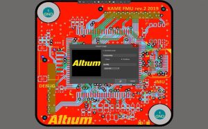
The three common approaches are:
- Import a bitmap image
- Import a DXF vector drawing
- Create a reusable custom PCB library footprint
Method 1: Import a Bitmap Image
Importing a bitmap is one of the simplest ways to add a basic logo to an Altium PCB. It is particularly suitable for simple monochrome graphics, text-based logos, symbols, and relatively uncomplicated artwork.
For PCB manufacturing, however, the quality of the original image is important. Very small details may be lost when the bitmap is converted into PCB geometry.
Step 1: Prepare the Logo Image
Prepare the logo as a monochrome bitmap, typically in BMP format when using Altium’s bitmap conversion workflow.
For the best result, use a high-contrast image with clear boundaries. Avoid unnecessary gradients, shadows, and very fine details.
Step 2: Open the PCB File
Launch Altium Designer and open the PCB document where you want to place the logo.
Make sure you are working on the correct board and have saved a backup before making significant design changes.
Step 3: Open the Bitmap Conversion Tool
In Altium Designer, access the bitmap conversion/import function through the appropriate Tools menu.
The exact menu wording may vary between Altium Designer versions, so use the bitmap conversion feature available in your installed version.
Step 4: Select the Bitmap File
When the file selection window appears, choose the prepared logo image.
Altium will convert the bitmap into PCB design objects that can be placed on the board.
Step 5: Select the Target Layer
Select the layer where the logo will be placed.
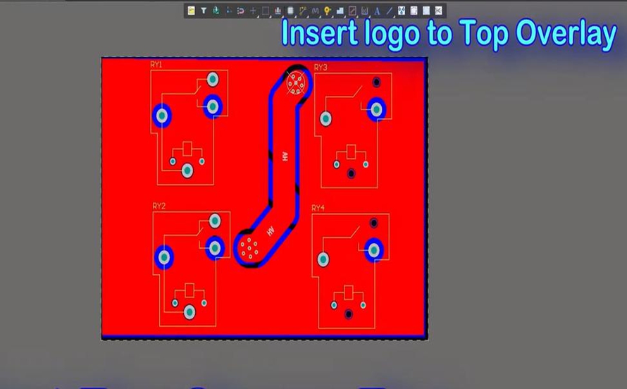
For most branding applications, the Top Overlay or Bottom Overlay layer is commonly used because these layers are associated with the PCB silkscreen.
A copper layer can also be used when a logo needs to be created as actual copper geometry. However, copper artwork must follow the same clearance and manufacturing rules as other copper features.
Step 6: Adjust the Image Parameters
Adjust parameters such as scaling, pixel size, and resolution as required.
Preview the converted artwork before placing it on the PCB. If the logo contains very fine lines or small characters, simplify the image before importing it.
Step 7: Place the Logo
Once the converted graphic looks correct, place it on the PCB and position it according to your design requirements.
Check the distance between the logo and nearby components, pads, traces, vias, and board edges.
Method 2: Import a DXF File
A DXF file is particularly useful when you need accurate vector geometry, clean outlines, or precise scaling.
Unlike a bitmap, a DXF file contains vector-based geometric information. This makes it useful for logos consisting of lines, arcs, outlines, and other geometric elements.
DXF is often a good choice when a logo needs to maintain its proportions while being scaled to different sizes.
Step 1: Prepare the DXF File
First, create or convert the logo into a compatible DXF file.
You can create the artwork in suitable CAD or vector-design software and export it as DXF.
Before exporting, simplify unnecessary geometry and confirm that the drawing uses the correct units and scale.
Step 2: Open the PCB Document
Open the target PCB file in Altium Designer.
It is recommended to save the current design before importing external geometry.
Step 3: Import the DXF File
Use the appropriate import command in Altium Designer to import the DXF/DWG drawing.
Depending on the Altium Designer version and workflow, the command location and dialog options may differ.
Step 4: Select the Target Layer
Choose the layer where the logo should be placed.
For a traditional printed logo, an overlay/silkscreen layer is usually appropriate. If the logo is intended to become copper, select the appropriate copper layer and verify the required clearances.
Step 5: Position and Scale the Logo
After importing the DXF geometry, position the logo on the PCB.
Check:
- Overall dimensions
- Scale
- Rotation
- Board-edge clearance
- Component clearance
- Line width
- Spacing between geometric elements
You can also inspect the result using Altium’s 2D and 3D views to verify how the logo will appear on the finished PCB.
Method 3: Create a Custom PCB Library Footprint
If you plan to use the same logo on multiple PCB projects, creating a reusable library footprint can be more efficient than repeatedly importing the artwork.
This method takes more initial setup but can save significant time when the same company logo or product identifier is used across multiple designs.
Step 1: Create a PCB Library
In Altium Designer, create a new PCB library through the appropriate File → New → Library → PCB Library workflow.
The exact interface may vary depending on the software version.
Step 2: Create the Logo Footprint
Open the footprint editor and create a dedicated footprint for the logo.
The logo can be drawn manually or created from imported bitmap/DXF geometry and then converted into suitable PCB objects.
Depending on the intended manufacturing process, the graphic can be constructed using overlay, copper, mechanical, or other appropriate layers.
Step 3: Save the Library
Save the PCB library so that the logo can be reused in future projects.
Use a clear and consistent naming convention, especially if your company has multiple product logos or identification marks.
Step 4: Place the Logo on a PCB
Once the logo footprint has been added to the library, it can be placed on a PCB in much the same way as a reusable component footprint.
This approach is particularly useful for manufacturers, engineering teams, and organizations that need consistent branding across multiple PCB designs.
Silkscreen Logo vs. Copper Logo
When adding a logo to a PCB, one important decision is whether to use the silkscreen or copper layer.
Silkscreen Logo
The silkscreen is the most common choice for PCB logos.
Advantages include:
- Clear visual identification
- No additional copper routing requirements
- Easy product and company branding
- Suitable for text and simple graphics
- Does not normally affect electrical routing
However, the logo must comply with the manufacturer’s minimum silkscreen line width, spacing, and character-size requirements.
Copper Logo
A logo can also be created using copper geometry.
Copper logos can provide a distinctive appearance and can be integrated directly into the conductive artwork. However, they must satisfy electrical clearances and other PCB fabrication requirements.
If a copper logo is placed near pads, traces, vias, or other conductive structures, verify that it does not create an unintended electrical connection or violate the manufacturer’s minimum spacing requirements.
Tips for Getting the Best PCB Logo
If you want your logo to look clean and professional after manufacturing, consider the following recommendations.
1. Keep the Logo Simple
Avoid extremely complicated graphics, tiny text, and very thin lines.
Fine details that look good on a computer screen may disappear during PCB production. Simple, high-contrast artwork generally produces more consistent results.
2. Follow the Manufacturer’s Silkscreen Rules
Before finalizing the logo, check your PCB manufacturer’s capabilities.
Important specifications may include:
- Minimum silkscreen line width
- Minimum character height
- Minimum spacing
- Registration tolerance
- Silkscreen-to-pad clearance
- Board-edge clearance
These specifications can vary between manufacturers and production processes.
3. Leave Adequate Clearance
Do not place the logo too close to pads, components, vias, board edges, or other critical features.
If the logo is printed over a solderable pad, the graphic may be partially removed or become difficult to read.
4. Check the Logo in 3D View
Use Altium’s 3D PCB view to inspect the approximate appearance of the logo on the finished board.
This is particularly helpful for identifying placement problems that may not be obvious in a 2D layout.
5. Run Design Rule Check
After placing the logo, run the Design Rule Check (DRC).
DRC can help identify clearance and other design violations. However, not every manufacturing issue will necessarily be detected by DRC, so the logo should also be checked against the PCB manufacturer’s fabrication specifications.
6. Verify the Final Manufacturing Data
Before releasing the design for PCB Manufacturing, confirm that the logo is present on the intended layer and that the generated manufacturing files correctly represent the artwork.
For example, verify the relevant Gerber or other manufacturing outputs to ensure that the logo has not been accidentally placed on the wrong layer or omitted from the fabrication package.
Common Mistakes When Adding PCB Logos
Several common mistakes can reduce the quality of the finished logo.
Using excessive detail: Very small features may not reproduce clearly.
Ignoring manufacturing limits: A logo that violates the manufacturer’s minimum line width or spacing may be modified or rejected during production.
Placing the logo over pads: This can interfere with solderable areas and reduce logo visibility.
Forgetting board-edge clearance: Artwork placed too close to the edge may be partially removed during fabrication or routing.
Failing to check the final files: The PCB layout may look correct while the exported manufacturing data contains an unexpected layer or geometry issue.
Conclusion
Adding a logo to a PCB is a simple but effective way to give a circuit board a professional and personalized appearance. If you understand how to add a logo in Altium PCB, you can use bitmap conversion, DXF import, or reusable PCB library graphics to integrate branding directly into your PCB Design.
For most standard applications, a simple silkscreen logo is practical and easy to manufacture. DXF-based vector artwork is useful when precise geometry and scaling are important, while a reusable PCB library footprint can save time when the same logo needs to be used across multiple projects.
Most importantly, the logo should be designed with PCB Manufacturing requirements in mind. Line width, spacing, clearance, artwork complexity, layer selection, and manufacturer capabilities all influence the final result.
With careful preparation and verification, a PCB logo can become more than a decorative element—it can provide clear product identification while reinforcing a consistent and professional brand image.