Hidden Costs of Cheap PCBs: PCB Design, PCB Manufacturing & SMT vs TH Guide
Every electronics product is developed under pressure to control costs and accelerate time to market. Engineering teams are often encouraged to reduce expenses wherever possible, and the PCB cost is frequently one of the first areas considered for savings.
At first glance, purchasing a low-cost PCB may seem like a sensible decision. If two manufacturers offer boards with apparently similar specifications but significantly different prices, choosing the cheaper quotation can appear financially attractive.
However, the lowest PCB price does not necessarily represent the lowest total cost.
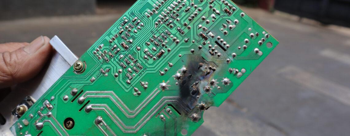
Low-cost or poorly controlled PCB manufacturing can introduce hidden expenses through lower yields, assembly problems, redesigns, testing failures, field returns, and premature product failures. These costs often appear much later—after prototypes have failed, production has been delayed, or products have already reached customers.
For engineering and procurement teams, understanding the real cost of a PCB is essential for building reliable, scalable, and commercially viable electronic products.
Why Are Cheap PCBs So Attractive?
During the design and procurement stages, PCB quotations can sometimes appear almost identical.
Two manufacturers may quote boards with the same:
- Board dimensions
- Layer count
- Copper weight
- Material family
- Surface finish
- Minimum trace and spacing requirements
- Via structures
- Production quantity
Yet the prices can still vary considerably.
Under budget pressure, it is easy to treat a PCB as a commodity and select the lowest quotation.
The problem is that a PCB is not simply a piece of laminate and copper. Manufacturing consistency, material quality, dimensional control, plating quality, solderability, electrical performance, inspection capability, and supplier process control can all affect the actual cost of the finished product.
Therefore, PCB purchasing decisions should consider total cost of ownership (TCO) rather than only the initial board price.
The Hidden Costs of Low-Cost PCB Manufacturing
1. Yield Loss and Assembly Failures
One of the first hidden costs of inconsistent PCB manufacturing is reduced production yield.
Dimensional variation, poor solderability, inadequate plating, solder-mask problems, pad defects, warpage, or other fabrication issues can interfere with PCB assembly.
For example, manufacturing variation can contribute to:
- Soldering defects
- Component placement problems
- Poor solder joints
- Opens or intermittent connections
- Assembly rework
- Scrap
- Production-line interruptions
Even a small reduction in first-pass yield can become expensive when thousands of PCB assemblies are produced.
The initial PCB quotation may be lower, but additional inspection, rework, replacement boards, and labor can quickly eliminate the apparent savings.
2. Signal Integrity and Electrical Performance Problems
PCB material selection and manufacturing consistency directly affect electrical performance, particularly in high-speed, RF, and impedance-controlled applications.
Important factors can include:
- Dielectric properties
- Copper thickness
- Trace geometry
- Dielectric thickness
- Layer registration
- Impedance control
- Surface roughness
- Via quality
For conventional low-speed circuits, small manufacturing variations may have little practical effect. However, high-speed interfaces, RF circuits, power electronics, and other demanding applications can be much more sensitive.
A board that appears acceptable during visual inspection may still produce signal-integrity problems during electrical testing.
This is one reason why PCB Design and PCB Manufacturing should be considered together rather than treated as completely independent activities.
3. Field Reliability Problems
The cost of a PCB does not end when the product leaves the factory.
A board that experiences premature failure in the field can generate much greater costs through:
- Warranty claims
- Product returns
- Service labor
- Replacement units
- Customer support
- Production recalls
- Reputation damage
- Lost engineering resources
Potential PCB reliability problems can include delamination, cracking, barrel failures, poor solderability, corrosion, and other manufacturing-related defects.
The risk can become more significant in products exposed to thermal cycling, vibration, humidity, chemicals, or other demanding operating conditions.
For these applications, PCB material selection and process control should be matched to the actual environmental and reliability requirements of the product.
4. Avoidable Redesigns
Another hidden cost is engineering time.
If a PCB does not perform consistently in manufacturing, engineering teams may need to modify the design to compensate for manufacturing limitations.
For example, engineers may need to:
- Modify footprints
- Change component placement
- Increase clearances
- Adjust trace geometry
- Change layer stackup
- Modify thermal structures
- Change via configurations
- Replace components
- Redesign problematic sections
A redesign can also trigger new PCB fabrication, assembly, testing, and validation activities.
As a result, the apparent savings from a cheaper PCB can be outweighed by additional engineering and production costs.
The Real Cost of a PCB Goes Beyond the Quotation
Many engineering teams eventually discover that PCB cost is not simply the price paid to the fabricator.
The actual cost may include:
PCB price + assembly cost + inspection + rework + scrap + engineering changes + testing + logistics + warranty + field failure risk
This does not mean that the most expensive PCB is automatically the best choice. Instead, the purchasing decision should balance price against the technical and production requirements of the application.
A cost-effective PCB is one that meets the required specifications consistently without creating unnecessary downstream expenses.
Quality Investment Can Reduce Total Product Cost
Investing in appropriate PCB quality can produce savings throughout the product lifecycle.
Consistent manufacturing can help improve:
- First-pass yield
- Assembly efficiency
- Electrical performance
- Product reliability
- Production predictability
- Time to market
- Long-term serviceability
The objective is not to purchase unnecessarily expensive materials or manufacturing processes. Instead, the goal is to select the appropriate combination of materials, tolerances, processes, inspection, and quality controls for the application.
For example, a basic consumer product may not require the same PCB material or manufacturing controls as an aerospace, medical, automotive, RF, or high-speed communication product.
Designing for Long-Term Manufacturing Success
The hidden cost of a cheap PCB can extend far beyond the purchase price.
A low initial quotation may eventually result in:
- Lost engineering time
- Production delays
- Higher assembly costs
- Increased scrap
- Additional testing
- Redesign cycles
- Field failures
- Missed market opportunities
This is why Design for Manufacturing (DFM) and supplier evaluation should be incorporated into the engineering process before production begins.
A capable PCB manufacturer should be able to communicate manufacturing limitations, identify potential risks, and help engineers develop a practical path from prototype to production.
SMT vs TH Assembly: Choosing the Right PCB Assembly Technology
PCB manufacturing does not end with bare-board fabrication. The assembly method used to attach components also has a major influence on product cost, density, reliability, and manufacturability.
The two fundamental component-assembly technologies are:
- Surface Mount Technology (SMT)
- Through-Hole (TH) Assembly
Most modern electronic products use SMT extensively, while TH components remain important for applications requiring mechanical strength, specialized component packages, or particular thermal and electrical characteristics.
The decision is therefore not simply SMT versus TH. In many products, the most practical solution is a combination of both technologies.
How Through-Hole Assembly Works
In Through-Hole Assembly, component leads pass through drilled holes in the PCB and are soldered to pads on the opposite side or otherwise connected according to the component and assembly design.
The leads provide a mechanical connection that can be advantageous for components exposed to physical stress.
TH assembly is commonly used for components such as:
- Board-to-board connectors
- Wire connectors
- Terminal blocks
- Switches
- Large transformers
- Certain power components
- Components subject to mechanical loads
Wave soldering is a common production method for suitable through-hole assemblies. The PCB passes over molten solder so that exposed solderable areas are wetted.
Selective soldering may be used when only specific through-hole locations need to be soldered, particularly on assemblies that also contain SMT components that should not be exposed to a conventional wave-soldering process.
How SMT Assembly Works
Surface Mount Technology (SMT) attaches components directly to solder pads on the PCB surface.
Instead of requiring leads to pass through drilled holes, SMT components are placed onto solder paste deposited on their pads and are typically soldered using a controlled reflow process.
A typical SMT process includes:
- Solder-paste printing
- Solder-paste inspection
- Component placement
- Reflow soldering
- Automated optical inspection
- Additional inspection or testing where required
SMT components are generally smaller than comparable through-hole components, allowing engineers to achieve higher component density and use both sides of the PCB.
Because SMT assembly can be highly automated, it is particularly suitable for modern high-density electronic products and volume production.
Key Differences Between SMT and TH Assembly
PCB Space and Component Density
SMT generally provides a major advantage when board space is limited.
Because SMT components are mounted directly on the surface, they can be placed at relatively high density, and both sides of a PCB can be populated.
Through-hole components require drilled holes and typically consume additional routing area around those holes. This can limit routing flexibility, particularly on dense multilayer boards.
For compact products, SMT is therefore often the primary assembly technology.
Mechanical Strength
Through-hole connections can provide strong mechanical anchoring because the component leads pass through the PCB.
This can be particularly useful for:
- Frequently inserted connectors
- Large switches
- Mechanical interfaces
- Components exposed to vibration
- Components subjected to repeated physical stress
However, mechanical reliability depends on the complete component, PCB, solder joint, mounting structure, and application environment—not simply whether the component uses TH or SMT.
Thermal Performance
Through-hole leads can sometimes provide an additional thermal path into the PCB.
This can be useful for certain power components, although thermal performance ultimately depends on the entire thermal design, including copper area, thermal vias, heatsinks, component package, PCB material, and airflow.
SMT components can also provide excellent thermal performance when appropriately designed, particularly when exposed pads and thermal vias are used.
Therefore, TH should not automatically be considered a superior thermal solution.
Cost and Production Speed
SMT is highly compatible with automated production.
Modern pick-and-place equipment can place large numbers of SMT components rapidly, while automated solder-paste printing and reflow provide a repeatable assembly process.
TH assembly can require additional insertion and soldering operations, depending on the component and production process.
For high-volume products, minimizing unnecessary TH components can simplify manufacturing. However, replacing a mechanically necessary TH component with SMT solely to reduce assembly cost may not be appropriate.
The optimal choice depends on the product requirements and production volume.
Component Availability
Many modern integrated circuits, resistors, capacitors, sensors, and other electronic components are primarily available in SMT packages.
Through-hole components remain available across many categories, particularly connectors, switches, terminal blocks, power components, and components designed for mechanical robustness.
Component availability should therefore be evaluated during PCB Design, especially for products expected to remain in production for many years.
Mixed-Technology PCB Assembly
Many commercial electronic products use both SMT and TH components.
A typical mixed-technology PCB might use SMT for:
- Integrated circuits
- Resistors
- Capacitors
- Small signal components
- Sensors
- Memory devices
while using TH for:
- Board connectors
- Power-entry terminals
- Large connectors
- Mechanically stressed components
- Selected high-power components
This approach combines the density and automation advantages of SMT with the mechanical advantages of TH where they are actually needed.
Mixed-technology assembly requires careful planning during the DFM stage.
The manufacturing sequence depends on the specific component arrangement, soldering process, PCB orientation, and equipment. In many conventional assemblies, SMT reflow is performed before through-hole soldering, but the exact process should be established with the assembly manufacturer.
If wave soldering is used, the PCB layout must also consider which SMT components are exposed to the solder wave and whether component orientation, spacing, thermal conditions, and solderability are suitable.
How to Choose Between SMT and TH
When selecting an assembly technology, consider the following questions:
Is the component available only in an SMT package?
If the required device is only available as an SMT component, the choice may already be determined.
Does the component experience mechanical stress?
For connectors, switches, terminals, or other components subject to repeated mechanical loads, TH may provide useful mechanical anchoring.
Is PCB space limited?
If the product requires high component density or compact dimensions, SMT is generally advantageous.
Will the product experience vibration or shock?
The complete mechanical design should be evaluated. TH components may be appropriate for specific mechanically stressed interfaces, but the PCB mounting structure and enclosure are also important.
Is the product manufactured in high volume?
High-volume manufacturing often benefits from highly automated SMT assembly. Nevertheless, required TH components can still be incorporated into an efficient mixed-technology process.
Does the component have thermal requirements?
Evaluate the complete thermal path rather than choosing SMT or TH based only on package type.
What does the EMS manufacturer recommend?
The assembly supplier can evaluate component placement, stencil design, soldering processes, testability, panelization, and production volume to determine the most practical manufacturing approach.
How PCB Design Influences Assembly Cost
Assembly technology should not be treated as an afterthought.
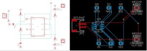
During PCB Design, engineers should consider:
- Component package selection
- Component orientation
- Component spacing
- Pad geometry
- Thermal pads
- Fiducials
- Test points
- Board-edge clearance
- Via placement
- Panelization
- SMT and TH interaction
- Inspection accessibility
- Rework requirements
These factors directly influence PCB Manufacturing and PCB assembly efficiency.
For example, reducing unnecessary TH components can simplify the manufacturing process, while poorly positioned components may increase inspection or rework requirements.
Similarly, selecting a component package only because it is inexpensive can create assembly difficulties if the package is difficult to source, inspect, place, or solder.
How Kingda Can Help Optimize PCB Manufacturing
For engineering teams, choosing a PCB supplier should involve more than comparing quotations.
Kingda can support customers by considering manufacturing requirements together with PCB design, assembly, component sourcing, and production objectives.
An effective manufacturing review can help identify potential risks related to:
- PCB material selection
- Layer stackup
- Trace and spacing requirements
- Via structures
- Surface finish
- Component footprints
- Assembly processes
- SMT/TH technology
- Testing
- Production volume
The goal is to establish a practical manufacturing solution that balances cost, quality, performance, and production requirements.
Practical PCB Cost-Saving Strategy
Instead of simply selecting the cheapest PCB quotation, engineering and procurement teams can use the following approach:
1. Define technical requirements
Identify the electrical, mechanical, thermal, environmental, and reliability requirements of the product.
2. Perform DFM analysis
Review the design with the intended PCB manufacturer before production.
3. Evaluate the complete BOM
Consider component cost, availability, lifecycle, package type, and assembly requirements.
4. Compare total manufacturing cost
Include fabrication, assembly, inspection, testing, rework, scrap, tooling, and logistics where applicable.
5. Select the appropriate assembly technology
Use SMT, TH, or mixed technology according to actual product requirements.
6. Validate the manufacturing process
Use prototype and pilot production to identify problems before volume manufacturing.
7. Monitor production yield
A slightly higher PCB price may be economically justified if it significantly improves manufacturing yield and reduces downstream costs.
Final Takeaways
The cheapest PCB quotation is not necessarily the lowest-cost manufacturing solution.
The true cost of a PCB includes much more than the initial purchase price. Yield loss, assembly defects, electrical performance problems, redesigns, testing, field failures, and production delays can all increase the total cost of an electronic product.
At the same time, choosing the right PCB assembly technology is equally important.
SMT provides high component density, strong automation potential, and excellent suitability for modern electronic products. TH assembly remains valuable where mechanical strength, specialized components, or specific application requirements justify its use. For many products, mixed-technology assembly provides a practical balance.
Ultimately, successful PCB Design should consider PCB Manufacturing from the beginning. By integrating DFM, component availability, assembly technology, testing, and supplier capabilities into the design process, engineering teams can reduce avoidable costs while improving manufacturing consistency and product reliability.
The goal should not be the cheapest PCB.
The goal should be the right PCB at the right total cost for the product’s technical and manufacturing requirements.