Surface Mount Technology (SMT) is the dominant assembly method used in modern PCB assembly. Unlike traditional through-hole technology (THT), SMT mounts electronic components directly onto solder pads on the surface of a printed circuit board rather than inserting component leads through drilled holes.
The widespread adoption of SMT PCB assembly has made it possible to develop smaller, lighter, faster, and more functionally dense electronic products. From smartphones and computers to automotive electronics, telecommunications equipment, medical devices, and industrial control systems, SMT plays a critical role in modern electronics manufacturing.
For manufacturers, however, successful SMT assembly involves much more than placing small components onto a PCB. Solder paste printing, component placement accuracy, reflow soldering, PCB design, stencil design, inspection, testing, and DFM optimization all influence final assembly quality.
As an experienced PCB manufacturer and PCB assemblyider, Kingda provides PCB prototype manufacturing, quick-turn PCB prototyping, and PCB assembly solutions to support customers from initial design validation through production.
What Is Surface Mount Technology?
Surface Mount Technology (SMT) is a PCB assembly technology in which electronic components are mounted directly onto the surface pads of a printed circuit board.
In a typical SMT assembly process, solder paste is first deposited onto designated PCB pads using a stencil. Automated pick-and-place equipment then positions Surface Mount Devices (SMDs) onto the solder paste. The assembled PCB subsequently passes through a controlled reflow soldering process, where the solder melts and forms mechanical and electrical connections between the components and PCB.
Compared with traditional through-hole assembly, SMT manufacturing offers several important advantages, including higher component density, better suitability for miniaturized products, faster automated production, and efficient use of PCB surface area.
Modern SMT is widely used in:
- Consumer electronics
- Automotive electronics
- Industrial automation
- Telecommunications equipment
- Medical electronics
- IoT devices
- Computer and networking equipment
- Power electronics
- Aerospace and high-reliability electronics
For products requiring compact dimensions and high circuit density, SMT PCB assembly is often the primary manufacturing technology.
SMT vs. SMD: What Is the Difference?
The terms SMT and SMD are closely related but describe different things.
SMT refers to the technology and manufacturing process used to mount components onto a PCB.
SMD refers to the electronic components designed to be mounted using that technology.
| Term | Full Name | Meaning | Examples |
|---|---|---|---|
| SMT | Surface Mount Technology | A PCB assembly method for mounting components directly onto PCB surface pads | Solder paste printing, pick-and-place, reflow soldering |
| SMD | Surface Mount Device | An electronic component designed for surface mounting | Chip resistors, MLCCs, QFN, BGA, QFP |
In simple terms, SMT is the assembly technology, while SMD is the component.
Advantages of Surface Mount Technology
The continued adoption of SMT assembly is largely driven by its ability to support miniaturization, automation, and high-density PCB designs.
Higher Component Density
SMD components generally require less PCB area than comparable through-hole components. This allows engineers to place more functions within the same board size.
High-density packages such as BGA, QFN, CSP, LGA, and fine-pitch QFP further increase the available circuit density.
Smaller and Lighter PCB Assemblies
Because SMT components do not require large through-holes and long component leads, PCB layouts can be more compact.
This is particularly important for smartphones, wearable electronics, portable medical devices, IoT products, and other space-constrained applications.
High-Speed Automated Manufacturing
Modern SMT production lines can automatically perform solder paste printing, component placement, reflow soldering, inspection, and other manufacturing operations.
Automation improves process repeatability and reduces dependence on manual component placement.
Better Suitability for High-Frequency Applications
The short electrical paths associated with many SMT packages can help reduce parasitic inductance and capacitance.
This makes SMT suitable for many high-speed digital, RF, telecommunications, and high-frequency PCB applications, although signal integrity ultimately depends on the complete PCB stackup, routing, materials, package design, and interconnect structure.
Support for Advanced IC Packages
Many modern integrated circuit packages are specifically designed for surface mounting.
Examples include:
- SOIC
- QFP
- QFN
- BGA
- CSP
- LGA
- TQFP
These packages support increasingly complex electronic designs while maintaining relatively compact footprints.
Efficient Automated Inspection
SMT production can be integrated with SPI, AOI, X-ray inspection, ICT, flying probe testing, and functional testing.
A properly designed inspection strategy allows manufacturers to detect process problems at different stages of production.
SMT PCB Assembly Process
A typical SMT PCB assembly process consists of several interconnected stages. The exact workflow can vary according to PCB design, component types, production volume, and testing requirements.
1. Solder Paste Printing
The first major step is solder paste printing.
A stainless-steel stencil is aligned with the PCB, and solder paste is deposited onto the required surface-mount pads.
The quality of solder paste printing has a direct effect on solder joint reliability. Excessive solder paste may cause bridging, while insufficient paste can result in weak joints or open connections.
Important factors include:
- Stencil thickness
- Aperture dimensions
- Squeegee pressure
- Printing speed
- Paste viscosity
- PCB pad geometry
- Stencil-to-board alignment
- Environmental conditions
For fine-pitch and miniature components, stencil aperture design becomes especially important.
2. Solder Paste Inspection (SPI)
After solder paste printing, Solder Paste Inspection (SPI) can be used to measure the deposited solder paste.
Modern 3D SPI systems can evaluate parameters such as:
- Paste volume
- Paste height
- Paste area
- X-Y offset
- Deposit shape
- Printing consistency
SPI provides early process feedback before components are placed.
For example, if the solder paste volume gradually decreases across a production run, the manufacturing process can be investigated before the issue results in large numbers of defective assemblies.
3. Pick-and-Place Assembly
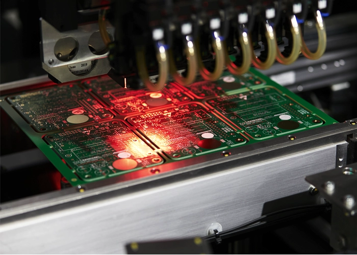
After solder paste inspection, automated pick-and-place machines place SMD components onto the PCB.
The placement system uses the assembly data to determine:
- Component reference
- X-Y coordinates
- Rotation angle
- Component package
- Feeder position
- Placement sequence
Components can range from relatively large connectors and IC packages to miniature chip resistors and capacitors.
Accurate PCB fiducials and properly prepared component libraries are important for achieving reliable placement.
4. Reflow Soldering
After component placement, the PCB enters a reflow oven.
The board passes through controlled temperature zones. The solder paste gradually transitions through preheat, soak, reflow, and cooling stages.
During the reflow stage, the solder melts and forms the electrical and mechanical connection between the SMD component and PCB pad.
A properly developed reflow profile should consider:
- Solder alloy
- PCB thickness
- Component thermal sensitivity
- PCB material
- Copper distribution
- Component density
- Package type
- Thermal mass
An unsuitable thermal profile can contribute to soldering defects, component damage, insufficient wetting, or excessive voiding.
5. Post-Reflow Inspection
After reflow, the assembled PCB is inspected to identify manufacturing defects.
Common inspection technologies include:
Automated Optical Inspection (AOI) checks visible features such as component presence, orientation, placement accuracy, and accessible solder joints.
X-ray Inspection (AXI) can inspect hidden solder connections beneath packages such as BGA and QFN.
Manual Visual Inspection can supplement automated inspection for specific workmanship requirements or complex assemblies.
6. Electrical and Functional Testing
Depending on product requirements, additional PCBA testing may include:
- Flying Probe Testing
- In-Circuit Testing (ICT)
- Functional Circuit Testing (FCT)
- Continuity testing
- Insulation testing
- Programming and firmware verification
- Power-on testing
The appropriate testing strategy depends on the product’s complexity, production volume, risk level, and customer requirements.
SMT Components and Package Sizes
Passive SMD Components
Passive components are among the most frequently used SMT components.
Common examples include:
- Resistors
- Ceramic capacitors
- Tantalum capacitors
- Inductors
- Ferrite beads
Common chip component sizes include:
| Package | Approximate Dimensions |
|---|---|
| 01005 | 0.4 × 0.2 mm |
| 0201 | 0.6 × 0.3 mm |
| 0402 | 1.0 × 0.5 mm |
| 0603 | 1.6 × 0.8 mm |
| 0805 | 2.0 × 1.25 mm |
| 1206 | 3.2 × 1.6 mm |
Smaller packages can increase circuit density, but they also place greater demands on PCB footprint design, stencil printing, component placement, inspection, and rework.
SMT IC Packages
Modern SMT PCB assembly supports a broad range of integrated circuit packages.
Common packages include:
- SOIC — Small Outline Integrated Circuit
- QFP — Quad Flat Package
- QFN — Quad Flat No-Lead
- BGA — Ball Grid Array
- TQFP — Thin Quad Flat Package
- LQFP — Low-Profile Quad Flat Package
- CSP — Chip Scale Package
- LGA — Land Grid Array
Package selection depends on electrical performance, thermal requirements, available PCB space, pin count, mechanical requirements, and manufacturing capability.
Component Orientation and Polarity
Certain SMD components are polarized and must be installed in the correct orientation.
Examples include:
- Diodes
- LEDs
- Tantalum capacitors
- Electrolytic capacitors
- Certain ICs and connectors
Incorrect polarity can cause circuit malfunction or component damage.
Therefore, polarity indicators should be clearly defined in the PCB design and assembly documentation. Automated placement equipment and inspection systems should also verify component orientation during production.
SMT vs. Through-Hole Technology
Both SMT and Through-Hole Technology (THT) remain important PCB assembly methods. The appropriate technology depends on the application and component requirements.
| Aspect | SMT | Through-Hole Technology |
|---|---|---|
| Component mounting | Components are mounted directly onto PCB surface pads | Leads pass through drilled PCB holes |
| Component density | High | Generally lower |
| Board size | Suitable for compact designs | Requires additional space for holes and pads |
| Automation | Highly suitable for automated assembly | Can use automated insertion, selective soldering, wave soldering, or manual assembly |
| Mechanical strength | Suitable for most electronic applications; depends on package and design | Often advantageous for mechanically stressed components |
| High-frequency applications | Generally well suited | Longer leads may introduce additional parasitic effects |
| Typical applications | Compact electronics, communications, automotive, industrial electronics | Connectors, transformers, large components, mechanically stressed parts |
| Double-sided assembly | Highly suitable | More design constraints |
| Production efficiency | High for many medium- and high-volume applications | Depends strongly on component and soldering process |
When Should You Choose SMT?
SMT assembly is generally appropriate when:
- The PCB needs to be compact and lightweight.
- High component density is required.
- The design uses BGA, QFN, CSP, or fine-pitch IC packages.
- Automated assembly is preferred.
- Both PCB sides contain components.
- High-speed or high-frequency performance is important.
- Medium- or high-volume production is expected.
When Should You Choose Through-Hole?
Through-hole components may be appropriate when:
- Strong mechanical retention is important.
- The assembly contains large connectors.
- Components experience significant mechanical stress.
- Large transformers or power components are required.
- The product requires specific through-hole components.
- Selective soldering or manual assembly is practical for the production volume.
Many modern products use a mixed SMT and THT assembly process, combining the advantages of both technologies.
SMT Assembly Design Guidelines and DFM Checklist
Good PCB design has a significant impact on SMT manufacturing efficiency, assembly quality, and production cost.
Before sending a design to manufacturing, engineers should perform a comprehensive Design for Manufacturing (DFM) review.
1. Optimize PCB Footprints
Use appropriate land patterns and ensure that component footprints match the manufacturer’s assembly requirements.
Incorrect footprints can result in:
- Solder bridges
- Opens
- Component misalignment
- Insufficient solder joints
- Tombstoning
2. Optimize Solder Mask Clearance
Fine-pitch components require adequate spacing between pads and solder mask openings.
Improper solder mask design can increase the risk of solder bridging.
3. Optimize Stencil Apertures
Stencil openings should be designed according to pad geometry, component pitch, package type, and solder paste requirements.
The same aperture strategy should not necessarily be applied to every component.
4. Provide Clear Polarity Markings
Ensure that polarity and pin-one indicators are clearly visible.
This helps prevent incorrect component orientation during both automated assembly and manual rework.
5. Use Fiducials
Global and local fiducials can improve machine vision alignment, particularly for dense or fine-pitch PCB designs.
6. Maintain Adequate Component Spacing
Sufficient spacing between components helps reduce:
- Placement interference
- Rework difficulty
- Inspection problems
- Soldering defects
- Mechanical interference
Component spacing should be determined based on the package type, assembly equipment, rework requirements, and PCB design.
7. Consider PCB Edge Clearance
Components should be positioned with sufficient clearance from the PCB edge to accommodate panelization, depanelization, handling, fixtures, and assembly equipment.
8. Avoid Silkscreen Over Pads
Reference designators and other silkscreen markings should not interfere with solder pads or component contacts.
9. Add Test Points
Accessible test points for important power rails, communication interfaces, programming signals, and critical nets can simplify electrical testing and troubleshooting.
10. Verify Component Availability
Before production, verify:
- Manufacturer part number
- Package
- Component lifecycle
- Availability
- Approved alternatives
- Electrical specifications
- BOM consistency
Component availability should be considered during design to reduce supply-chain interruptions.
11. Review Panelization
Panelization should be optimized according to:
- PCB dimensions
- Component distribution
- Tooling requirements
- Board-edge clearance
- Depanelization method
- Assembly equipment
Good panel design can improve manufacturing efficiency and reduce handling costs.
Common SMT Soldering Defects and Prevention
Even automated SMT assembly can produce defects if material quality, PCB design, printing, placement, or reflow conditions are not properly controlled.
| Defect | Common Causes | Prevention |
|---|---|---|
| Tombstoning | Uneven heating or unequal solder volume | Balance pad design, stencil apertures, and reflow profile |
| Solder Bridging | Excess solder paste or insufficient pad spacing | Optimize stencil design and printing parameters |
| Cold Solder Joint | Insufficient heat or poor wetting | Optimize reflow profile and verify solder paste condition |
| Component Misalignment | Placement error or inaccurate fiducials | Calibrate placement equipment and improve board alignment |
| Open Joint | Insufficient solder or poor wetting | Check solder paste volume, pad finish, and component coplanarity |
| Solder Voiding | Flux entrapment or unsuitable thermal pad design | Optimize stencil design, paste selection, and reflow profile |
| Insufficient Solder | Low paste volume or poor transfer efficiency | Improve stencil aperture and printing parameters |
| Excessive Solder | Excessive paste deposition | Reduce aperture volume and optimize printing |
| Component Damage | Excessive thermal exposure or handling | Review reflow profile and material specifications |
A combination of SPI, AOI, X-ray inspection, electrical testing, and process monitoring can help identify the source of recurring SMT defects.
What Affects SMT Assembly Cost?
The cost of SMT PCB assembly depends on many factors rather than component count alone.
1. Component Count
A larger number of component placements generally increases machine runtime and manufacturing effort.
A board with 1,000 placements will normally require more placement time than a board with 200 placements, assuming other variables are comparable.
2. Component Package and Size
Fine-pitch and miniature components can increase manufacturing complexity.
Packages such as:
- BGA
- QFN
- CSP
- LGA
- 0201
- 01005
may require more precise placement, stencil design, inspection, or rework processes.
3. Number of Unique Components
A high number of unique part numbers can increase:
- Feeder setup
- Component preparation
- Machine changeovers
- Inventory management
- BOM management
Standardizing components where electrically and mechanically appropriate can improve manufacturing efficiency.
4. Single-Sided vs. Double-Sided Assembly
Double-sided SMT assembly generally requires additional process steps and handling compared with single-sided assembly.
The actual cost impact depends on component distribution, board design, production volume, and assembly process.
5. PCB Panelization
Efficient panelization can improve equipment utilization and reduce handling time.
Poor panelization may increase production waste and manufacturing complexity.
6. Inspection and Testing
Advanced inspection and testing can increase manufacturing costs but may be essential for high-reliability applications.
Possible processes include:
- SPI
- AOI
- X-ray Inspection
- Flying Probe Testing
- ICT
- FCT
- Reliability testing
The appropriate combination should be determined according to product risk and customer requirements.
7. Production Volume
Prototype and low-volume production often have higher unit costs because setup, programming, engineering, and preparation costs are distributed across fewer boards.
As production volume increases, these fixed costs can generally be distributed across more units.
Example: Why Component Count Does Not Tell the Whole Cost Story
Consider two PCB assemblies with similar board dimensions.
Board A contains 500 standard passive components and several conventional IC packages.
Board B contains only 250 components but includes multiple fine-pitch BGAs and QFNs and requires X-ray inspection.
Although Board B has fewer components, its manufacturing process may be more complex because of:
- Higher placement precision requirements
- More demanding stencil design
- Hidden solder joints
- Additional inspection
- Greater rework difficulty
- More complex process control
Therefore, SMT assembly cost should be evaluated based on the complete manufacturing process rather than component count alone.
What Files Are Needed for SMT PCB Assembly?
A professional PCB assembly manufacturer normally requires several files and documents before production.
Gerber Files
Gerber files provide the PCB fabrication information, including copper layers, solder mask, silkscreen, and other manufacturing data.
Bill of Materials (BOM)
The BOM should include:
- Manufacturer part number
- Quantity
- Reference designator
- Component description
- Package
- Approved alternatives where applicable
Pick-and-Place File
The CPL / XY file provides:
- Component coordinates
- Reference designators
- Rotation
- Side of PCB
- Component placement information
Assembly Drawing
An assembly drawing can clarify:
- Component orientation
- Polarity
- Special assembly requirements
- Mechanical restrictions
- Non-standard components
Testing Requirements
If the project requires ICT, FCT, flying probe testing, programming, or other verification, the corresponding requirements should be supplied before production.
Providing complete and accurate manufacturing data helps reduce engineering clarification and improves production efficiency.
SMT Quality Standards and IPC Guidelines
Professional SMT manufacturing commonly references IPC standards when defining PCB assembly workmanship, soldering processes, and component footprints.
Important standards include:
IPC-A-610
IPC-A-610 provides acceptability criteria for electronic assemblies, including component mounting, solder joints, and workmanship.
IPC-7351
IPC-7351 provides guidance for SMT land patterns and PCB footprints.
Following appropriate footprint guidelines helps improve manufacturability and soldering consistency.
IPC J-STD-001
IPC J-STD-001 establishes requirements for soldered electrical and electronic assemblies, including materials, processes, and soldering workmanship.
The applicable standard and acceptance class should be agreed between the customer and manufacturer based on the product’s intended use.
IPC Class 1
Class 1 generally applies to general electronic products where the primary requirement is basic functional performance.
IPC Class 2
Class 2 applies to dedicated-service electronic products where continued performance and extended service life are important.
Examples may include:
- Industrial equipment
- Telecommunications equipment
- Commercial electronics
- Networking equipment
IPC Class 3
Class 3 applies to high-reliability electronic products where continued performance is critical and the operating environment may be demanding.
Applications may include:
- Aerospace electronics
- Medical equipment
- Mission-critical systems
- Certain high-reliability industrial applications
The appropriate IPC class should be specified according to the product’s application and reliability requirements rather than selected solely according to industry category.
Kingda SMT PCB Assembly Solutions
Choosing the right PCB assembly partner is just as important as selecting the correct SMT process.
As an experienced PCB manufacturer and PCB assembly service provider, Kingda provides integrated manufacturing support for customers developing and producing electronic products.
PCB Prototype Manufacturing
Kingda provides PCB prototype manufacturing to help customers verify PCB designs before committing to larger production volumes.
Prototype manufacturing can help identify:
- PCB layout problems
- Component compatibility issues
- Assembly difficulties
- DFM concerns
- Electrical and functional issues
Quick-Turn PCB Prototyping
For new product development, quick-turn PCB prototyping helps shorten the design-validation cycle.
Customers can move from PCB design and engineering verification toward assembly and product validation more efficiently.
PCB Assembly Services
Kingda provides PCB assembly solutions covering the transition from bare PCB manufacturing to component assembly.
Depending on project requirements, the manufacturing workflow can incorporate:
- SMT assembly
- Through-hole assembly
- Mixed technology assembly
- Component sourcing
- DFM review
- Assembly inspection
- Electrical testing
- Functional verification
Support from Prototype to Production
One of the advantages of working with an integrated PCB and PCBA supplier is that design and manufacturing issues can be identified earlier.
Kingda supports customers from initial design validation and PCB prototyping through PCB assembly and production, helping establish a more consistent manufacturing workflow.
Engineering and DFM Support
A professional DFM review can identify potential manufacturing problems before production begins.
Typical review areas include:
- PCB footprint design
- Component spacing
- Stencil requirements
- Panelization
- Component availability
- Assembly orientation
- Test-point accessibility
- Manufacturing documentation
This early-stage engineering approach can reduce avoidable production problems and improve manufacturing efficiency.
How to Reduce SMT Assembly Costs
Cost optimization should not simply focus on reducing the assembly quotation. The goal is to reduce the total manufacturing cost while maintaining required quality and reliability.
Consider the following strategies:
- Optimize component selection to reduce unnecessary part-number diversity.
- Use standard package sizes where they meet electrical and mechanical requirements.
- Improve PCB panelization to maximize manufacturing utilization.
- Complete DFM review before production to prevent avoidable manufacturing defects.
- Optimize stencil design for efficient solder paste transfer.
- Verify BOM accuracy before component procurement.
- Select an appropriate inspection strategy based on product risk.
- Design accessible test points to simplify electrical testing.
- Plan component availability early to reduce production interruptions.
- Use the same manufacturing partner for PCB and PCBA where practical to simplify communication and process coordination.
Frequently Asked Questions About SMT
What is SMT in PCB assembly?
SMT, or Surface Mount Technology, is a PCB assembly method in which electronic components are mounted directly onto PCB surface pads instead of inserting leads through drilled holes.
What is the difference between SMT and SMD?
SMT refers to the assembly technology, while SMD refers to the surface-mount components used with that technology.
Is SMT better than through-hole assembly?
Neither technology is universally better. SMT is generally advantageous for compact, high-density, automated assemblies, while through-hole technology can provide useful mechanical retention for connectors, large components, and mechanically stressed applications.
Many products use both technologies in a mixed SMT/THT assembly.
What are the main SMT assembly steps?
The typical SMT process includes:
- Solder paste printing
- SPI
- Pick-and-place
- Reflow soldering
- AOI
- X-ray inspection where required
- Electrical testing
- Functional testing where required
What causes SMT soldering defects?
Common causes include:
- Incorrect stencil design
- Poor solder paste printing
- Incorrect component placement
- Improper PCB footprint
- Unsuitable reflow profile
- Component coplanarity problems
- PCB surface-finish issues
- Material or process variation
How can SMT assembly quality be improved?
A comprehensive approach should combine DFM review, controlled solder paste printing, accurate component placement, optimized reflow profiles, SPI, AOI, X-ray inspection where appropriate, and electrical or functional testing.
What information should I provide to an SMT assembly manufacturer?
At minimum, provide:
- Gerber files
- BOM
- Pick-and-place/CPL file
- Assembly drawings
- PCB specifications
- Component requirements
- Testing requirements
- Special manufacturing instructions
Providing complete and accurate documentation allows the manufacturer to evaluate manufacturability before production.
Conclusion
Surface Mount Technology (STM) has become a fundamental technology in modern electronics manufacturing because it supports compact PCB designs, high component density, automated production, and efficient manufacturing.
However, successful SMT PCB assembly depends on more than simply selecting SMD components. PCB footprints, stencil design, solder paste printing, component placement, reflow soldering, inspection, testing, and DFM all contribute to final product quality.
Manufacturers must also select the appropriate combination of SPI, AOI, X-ray inspection, flying probe testing, ICT, and FCT according to product complexity, production volume, reliability requirements, and application environment.
For companies developing new electronic products, Kingda provides, quick-turn PCB prototyping, and PCB assembly solutions, supporting customers from initial design validation through .
By combining sound PCB design practices with effective DFM review, controlled SMT manufacturing, appropriate inspection, and systematic testing, engineers can reduce manufacturing risks, improve assembly consistency, and build more reliable electronic products.