


Engineering Context
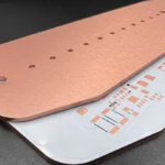
Ceramic printed circuit boards (Ceramic PCBs) represent a critical platform for next-generation electronics operating under extreme thermal, electrical, and environmental stress. Unlike conventional FR4 or metal-core PCB solutions, ceramic PCB technology leverages inorganic ceramic substrates to achieve exceptional thermal conductivity, dielectric strength, and phase stability across wide temperature ranges. These characteristics make ceramic PCBs indispensable in automotive radar, aerospace avionics, RF/mmWave communication systems, medical imaging, and industrial sensing. This article provides an engineer-oriented technical overview of ceramic PCB materials, dielectric behavior, stackup design, RF implementation, and validated reliability performance.
Core Engineering Challenges
As power density and operating frequency continue to increase, modern electronic systems face persistent challenges related to heat dissipation, signal integrity, and long-term reliability. In high-frequency RF PCB and mmWave systems, dielectric loss, insertion loss drift, and phase instability can directly degrade system accuracy. Traditional organic laminates suffer from moisture absorption, CTE mismatch, and material decomposition at elevated temperatures.
Ceramic PCBs address these limitations by eliminating organic constituents and introducing substrates with intrinsically high thermal conductivity and dielectric strength. However, engineers must carefully balance material selection, metallization methods, and stackup symmetry to mitigate EMI, control impedance, and ensure manufacturability at scale.
Material Science & Dielectric Performance
The performance of a ceramic PCB is fundamentally defined by its substrate material. Common ceramic materials include alumina (Al₂O₃), aluminum nitride (AlN), silicon nitride (Si₃N₄), and beryllium oxide (BeO). Each material exhibits unique thermal, mechanical, and dielectric characteristics.
Ceramic Material Parameter Comparison
| Material | Thermal Conductivity (W/m·K) | Dielectric Constant (1 MHz) | Bending Strength (MPa) | Relative Cost |
|---|---|---|---|---|
| Al₂O₃ (96%) | 24–28 | 9.8 | 350 | Low |
| Al₂O₃ (99.6%) | 28–35 | 9.9 | 400 | Low–Medium |
| AlN | 170–230 | 8.8 | 350 | High |
| Si₃N₄ | 70–90 | 8.0 | 700 | High |
| BeO | 250–300 | 6.7 | 230 | Very High |
Alumina remains the most widely used ceramic PCB material due to its cost-effectiveness and stable dielectric behavior. For high-power and mmWave PCB applications, AlN is preferred because its thermal conductivity rivals metals while maintaining electrical insulation. Ceramic substrates typically exhibit breakdown voltages exceeding 10–20 kV/mm and near-zero water absorption, enabling consistent electrical performance over time.
GOPCBA Case Study — Automotive Radar PCB
Industry Application: 77 GHz automotive radar sensor module
Customer Requirements
- High thermal conductivity substrate for power amplifier dissipation
- Stable dielectric constant for phase-critical mmWave operation
- Low insertion loss and controlled EMI radiation
- Reliability under thermal cycling and vibration
Engineering Challenges Initial FR4 and aluminum MCPCB solutions failed to meet phase stability and insertion loss targets at elevated temperatures. Thermal gradients caused frequency drift and degraded RF matching.
GOPCBA Solution GOPCBA implemented an AlN-based ceramic PCB using DPC (Direct Plated Copper) technology. A symmetrical multilayer stackup was optimized for impedance control and EMI suppression.
Measured Results
| Test Parameter | Target | Measured |
| Thermal Resistance | ≤1.2 °C/W | 0.9 °C/W |
| Insertion Loss @77 GHz | ≤2.0 dB | 1.6 dB |
| Phase Stability (-40–125°C) | ±2° | ±1.1° |
| EMI Margin | CISPR 25 | Pass |
Stackup Design & RF Implementation
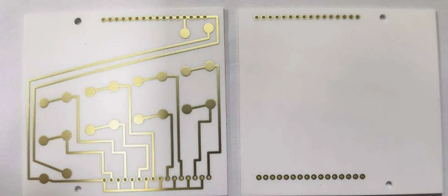
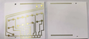
A typical ceramic PCB stackup integrates copper metallization directly bonded or plated onto the ceramic substrate. Common metallization technologies include DBC, DPC, thick-film, and thin-film processes.
Typical Ceramic PCB Stackup
| Layer | Material | Function |
| Top Copper | 1–2 oz Cu | RF signal / power routing |
| Ceramic Substrate | Al₂O₃ / AlN | Thermal spreading, dielectric isolation |
| Bottom Copper | Optional | Ground plane / heat spreading |
For RF PCB and mmWave designs, ceramic substrates offer low dielectric loss and excellent phase stability across temperature. HFSS and ADS simulations are used to model insertion loss, impedance uniformity, and EMI coupling. TDR measurements validate controlled impedance, while Thermal FEM simulations confirm junction temperature margins.
Environmental & Reliability Validation
Ceramic PCBs are qualified through rigorous environmental and mechanical testing to ensure long-term reliability.
Reliability Test Summary
| Test Type | Condition | Result |
| Thermal Cycling | -55°C to +150°C, 1000 cycles | Pass |
| High Humidity | 85°C / 85% RH, 1000 h | Pass |
| Vibration | Automotive & aerospace profiles | Pass |
| Solder Reflow | 260°C, multiple cycles | No delamination |
Due to their inorganic composition, ceramic PCBs demonstrate superior resistance to moisture, corrosion, and thermal fatigue compared to FR4 and MCPCB alternatives.
Engineering Summary & Contact
Ceramic PCB technology provides a robust foundation for electronics operating in extreme thermal, electrical, and environmental conditions. By combining high thermal conductivity, low-loss dielectric behavior, and outstanding phase stability, ceramic PCBs enable reliable RF PCB and mmWave PCB implementations that exceed the limitations of traditional substrates.
GOPCBA supports ceramic PCB design, simulation, prototyping, and volume manufacturing across automotive, aerospace, medical, and industrial sectors. Engineering teams seeking advanced thermal management and signal integrity solutions are encouraged to engage with GOPCBA for material selection and stackup optimization.