PCB Eight Discipline Problem Solving: Working a Problem to the End Electronics manufacturing has become a discipline of small details. Solder paste volumes, placement accuracy, temperature profiles and inspection limits all add up to the final result. This guide looks at PCB eight discipline problem solving from the perspective of…

PCB Debugging a New Board: Tools, Flow and Soldering A new board rarely works the first time it is powered, and the difference between a project that recovers in a day and one that loses a week is usually the debugging method rather than the fault. Bring-up on a fresh…
Lead-Free SMT PCB Design: Materials, Pads and Compatibility Lead-free assembly has been the default for consumer and industrial electronics for years, yet the design rules that support it are still applied inconsistently. A lead-free SMT PCB design is not simply a board assembled with a different alloy. The higher process…
Four-Layer PCB Design: From Schematic Capture to Routing A four-layer board is the first stackup that gives a designer a real ground plane, and the first where the order of the workflow starts to matter. On a two-layer board the layout can be adjusted almost indefinitely without changing the electrical…
PCB Gauge Repeatability for Inspection: A Factory-Floor Review Buyers and engineers often focus on the finished product and forget the production line behind it. In practice, most field failures can be traced back to process decisions made during assembly. Understanding PCB gauge repeatability for inspection gives you a practical advantage…
High-Speed PCB Layout: 20 Practical Questions Answered High-speed layout questions come up again and again because the answers depend on frequency, geometry and the behaviour of the return current rather than on a fixed rule. The twenty points below are the ones engineers ask most often, answered as briefly as…
PCB Design Workflow: From Netlist to Final Layout Schematic capture exists for a practical reason: it produces the netlist that the board layout is built from and establishes the basis for everything that follows. Once the netlist is available, the layout work itself is a sequence of decisions that run…
PCB Coverlay Versus Solder Mask: Two Ways to Cover a Flex Buyers and engineers often focus on the finished product and forget the production line behind it. In practice, most field failures can be traced back to process decisions made during assembly. Understanding PCB coverlay versus solder mask gives you…
PCB Rigid Flex Bend Radius: From Design to Repeatable Production Buyers and engineers often focus on the finished product and forget the production line behind it. In practice, most field failures can be traced back to process decisions made during assembly. Understanding PCB rigid flex bend radius gives you a…
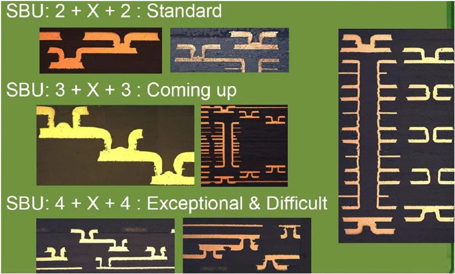
Via Drilling in Prototype Boards: Through, Blind and Buried Drilling is one of the largest single cost elements in a prototype order, and the type of hole chosen determines not only the price but the number of lamination cycles the panel has to survive. Understanding the three via types and…