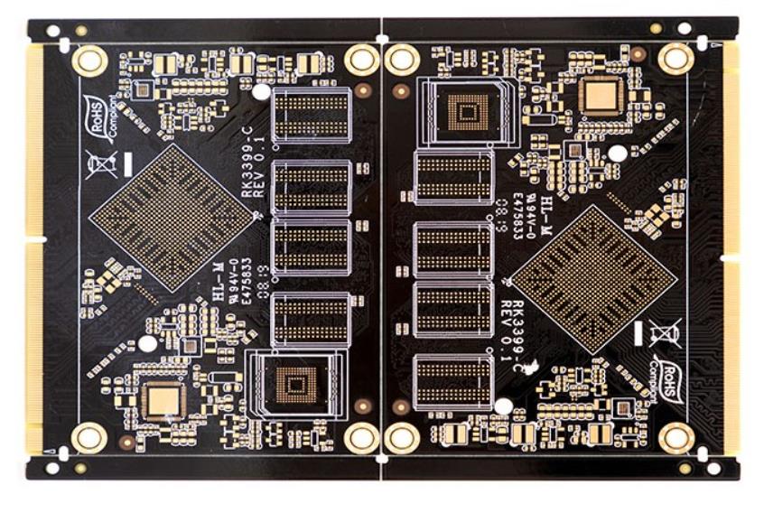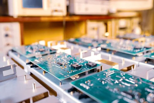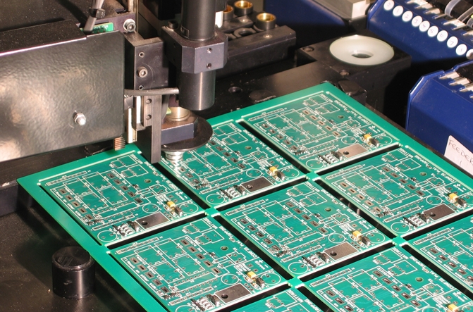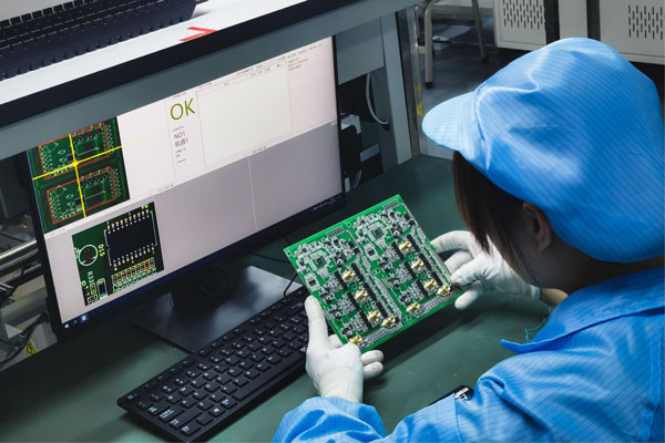
PCB Panel Array Design: Many Boards at Once Modern electronics depend on boards that are assembled correctly the first time. Every product – a phone, a charger, a medical instrument or an industrial controller – relies on thousands of solder joints that must conduct current for years. This article explains…

Preventing Tombstoning and Cold Joints at the Design Stage When a chip component stands up on one end after reflow, or a joint that looks complete turns out to be electrically open, the first suspects are usually the paste, the profile or the placement machine. Production data points somewhere else:…
PCB Solder Mask Dam Width: The Web Between Pads Electronics manufacturing has become a discipline of small details. Solder paste volumes, placement accuracy, temperature profiles and inspection limits all add up to the final result. This guide looks at PCB solder mask dam width from the perspective of a PCBA…
PCB Silkscreen Design Rules: Writing on the Board Buyers and engineers often focus on the finished product and forget the production line behind it. In practice, most field failures can be traced back to process decisions made during assembly. Understanding PCB silkscreen design rules gives you a practical advantage when…
PCB Via in Pad Filling: Filling the Hole Buyers and engineers often focus on the finished product and forget the production line behind it. In practice, most field failures can be traced back to process decisions made during assembly. Understanding PCB via in pad filling gives you a practical advantage…
PCB Heat Spreading Under a Part: Moving Heat Away A power component does not fail because the board is badly made. It fails because heat cannot leave the package fast enough. The copper under the part, the vias through the laminate and the airflow above the board decide how long…
PCB Panel Plating Process: Plating Before Etching Buyers and engineers often focus on the finished product and forget the production line behind it. In practice, most field failures can be traced back to process decisions made during assembly. Understanding PCB panel plating process gives you a practical advantage when you…
PCB Signal Layer Assignment: Which Layer Carries What Modern electronics depend on boards that are assembled correctly the first time. Every product – a phone, a charger, a medical instrument or an industrial controller – relies on thousands of solder joints that must conduct current for years. This article explains…
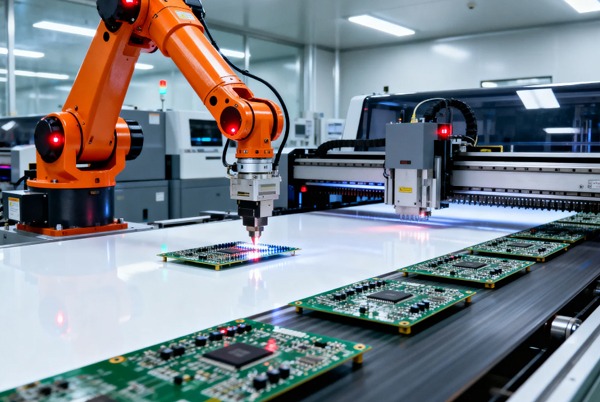
PCB Core and Prepreg Thickness: Building the Thickness Buyers and engineers often focus on the finished product and forget the production line behind it. In practice, most field failures can be traced back to process decisions made during assembly. Understanding PCB core and prepreg thickness gives you a practical advantage…
PCB Dielectric Constant Selection: Matching the Material Electronics manufacturing has become a discipline of small details. Solder paste volumes, placement accuracy, temperature profiles and inspection limits all add up to the final result. This guide looks at PCB dielectric constant selection from the perspective of a PCBA factory floor, covering…