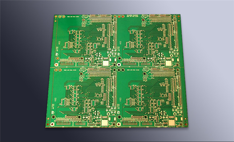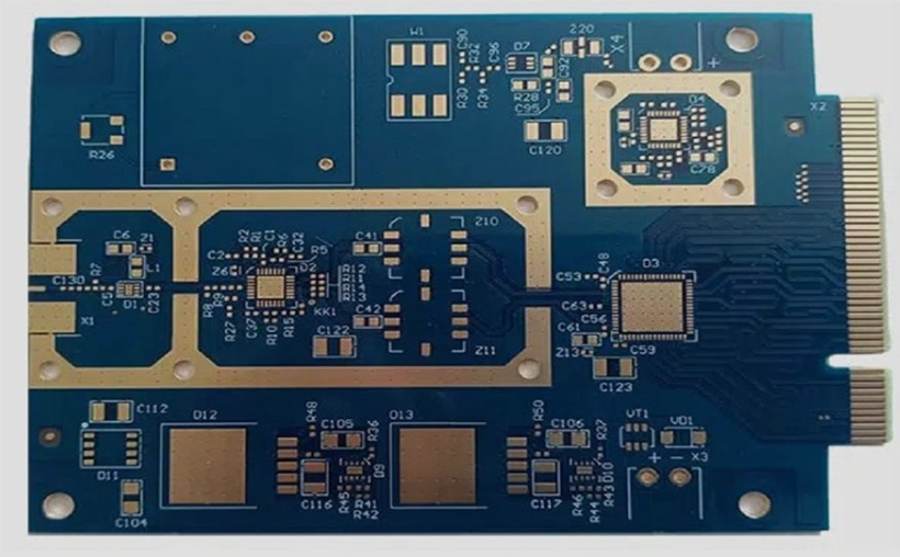
Impedance Coupon Design: 6 Rules for a Coupon You Can Trust An impedance coupon is a set of test traces built into the panel border that lets the fabricator and the customer measure the controlled impedance the process actually produced. A well built test coupon is the only practical way…

Skipped Deposits: Preparation, Placement and Process Control Skipped deposits are apertures that receive no paste at all, leaving a bare pad after the print. The defect is different from a deposit that is short or thin, because the failure is complete rather than partial, and the cause is usually a…
Graping Defect: 5 Causes in Solder Paste Reflow Graping is a reflow defect in which the paste on a pad turns into a cluster of small balls instead of one smooth fillet. The balls sit on the pad like a bunch of grapes, each one individually rounded, and the pad…
PCB Defect Pareto Data: A Practical Review for Manufacturing Teams Modern electronics depend on boards that are assembled correctly the first time. Every product – a phone, a charger, a medical instrument or an industrial controller – relies on thousands of solder joints that must conduct current for years. This…
PCB Defect Pareto Limits: A Factory-Floor Review Buyers and engineers often focus on the finished product and forget the production line behind it. In practice, most field failures can be traced back to process decisions made during assembly. Understanding PCB defect pareto limits gives you a practical advantage when you…
PCB Defect Pareto Maintenance: Practical Process Controls Modern electronics depend on boards that are assembled correctly the first time. Every product – a phone, a charger, a medical instrument or an industrial controller – relies on thousands of solder joints that must conduct current for years. This article explains PCB…
PCB Defect Pareto Setup: From Design to Repeatable Production Buyers and engineers often focus on the finished product and forget the production line behind it. In practice, most field failures can be traced back to process decisions made during assembly. Understanding PCB defect pareto setup gives you a practical advantage…
PCB Defect Pareto Defects: What Buyers and Engineers Should Check Modern electronics depend on boards that are assembled correctly the first time. Every product – a phone, a charger, a medical instrument or an industrial controller – relies on thousands of solder joints that must conduct current for years. This…
PCB Defect Pareto Standards: Design, Process, and Quality Notes Buyers and engineers often focus on the finished product and forget the production line behind it. In practice, most field failures can be traced back to process decisions made during assembly. Understanding PCB defect pareto standards gives you a practical advantage…
PCB Defect Pareto Training: Design, Process, and Quality Notes Buyers and engineers often focus on the finished product and forget the production line behind it. In practice, most field failures can be traced back to process decisions made during assembly. Understanding PCB defect pareto training gives you a practical advantage…