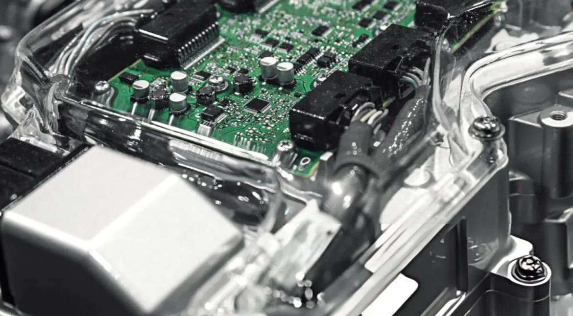
Solder Mask Curing: 6 Stages From UV Tack to Final Bake Solder mask curing is the sequence of tack dry, UV exposure and thermal bake that turns a printed liquid film into a hard, chemically resistant coating. Shorten a stage and the mask can pass a visual check while still…
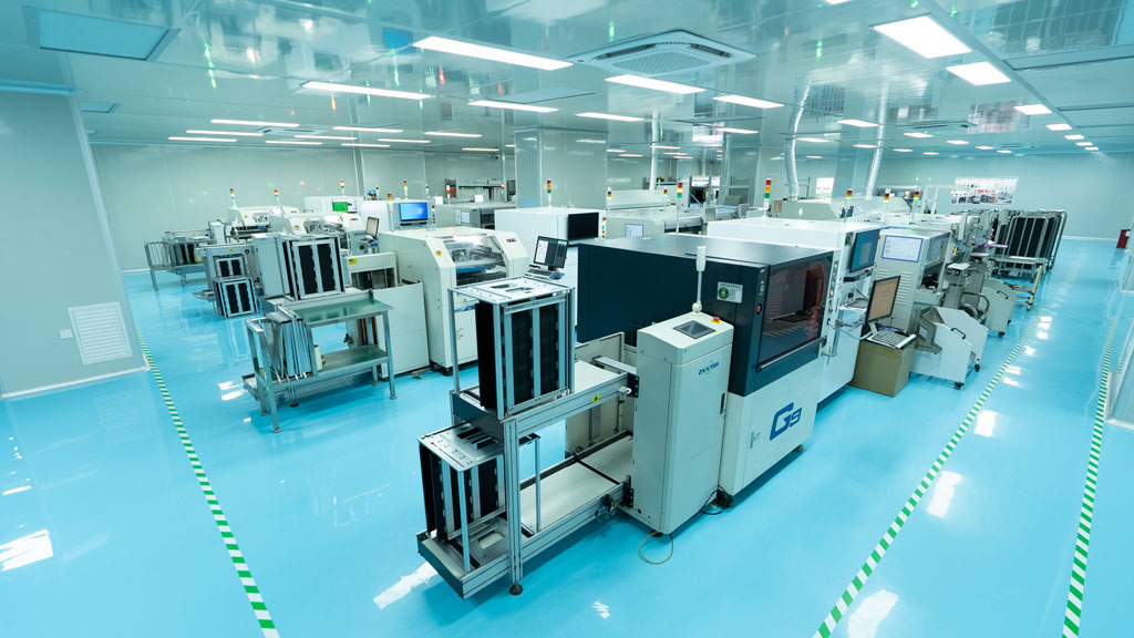
Pattern Plating on PCB: 7 Controls That Fix Copper Thickness Pattern plating is the electrolytic step that builds copper on the traces and inside the drilled holes after the plating resist has defined which areas will be plated. It follows the electroless copper that makes the hole walls conductive, and…
PCB Cycle Time Maintenance: A Factory-Floor Review Buyers and engineers often focus on the finished product and forget the production line behind it. In practice, most field failures can be traced back to process decisions made during assembly. Understanding PCB cycle time maintenance gives you a practical advantage when you…
Half Ounce Copper: Where 0.5 oz Foil Fits in a Stack-Up Half ounce copper is foil rolled to about 17.5 micrometres nominal thickness, half the weight of the standard one ounce foil. It is chosen when the design needs finer traces, a thinner finished board or a lighter panel, and…
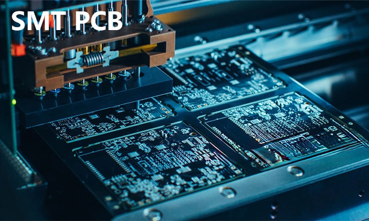
Pick Height on SMT Feeders: 5 Setup Rules Pick height is the Z position at which the vacuum nozzle meets the component inside the tape pocket. The machine closes the vacuum at that point and waits for a pressure switch or a flow sensor to confirm that a part is…
PCB Cycle Time Setup: From Design to Repeatable Production Modern electronics depend on boards that are assembled correctly the first time. Every product – a phone, a charger, a medical instrument or an industrial controller – relies on thousands of solder joints that must conduct current for years. This article…
PCB Cycle Time Defects: A Practical Manufacturing Guide Buyers and engineers often focus on the finished product and forget the production line behind it. In practice, most field failures can be traced back to process decisions made during assembly. Understanding PCB cycle time defects gives you a practical advantage when…
PCB Cycle Time Standards: Design and Assembly Considerations Electronics manufacturing has become a discipline of small details. Solder paste volumes, placement accuracy, temperature profiles and inspection limits all add up to the final result. This guide looks at PCB cycle time standards from the perspective of a PCBA factory floor,…
Brown Oxide: Design Rules and Process Limits Brown oxide treatment is the chemical step that grows a controlled copper oxide layer on inner layer copper so the prepreg can bond to it during lamination. The copper leaves the line with a matte, dark brown surface built from fine dendrites. That…
PCB Cycle Time Training: Process Details and Inspection Points Buyers and engineers often focus on the finished product and forget the production line behind it. In practice, most field failures can be traced back to process decisions made during assembly. Understanding PCB cycle time training gives you a practical advantage…