KingdaKingdaKingda

Call Us 24/7

+86-181-2376-9076

Send Us Mail

sales@gopcba.com

Our Location

Baoan District, Shenzhen, China

Language

  • enEnglish
    • fr France
    • itItalian
Kingda
  • Home
  • PCB Assembly
    • Prototype PCB Assembly
    • Turnkey PCB Assembly
    • Low Volume PCB Assembly
    • High Volume PCB Assembly
    • SMT PCB Assembly
    • Through Hole PCB Assembly
    • Mixed Technology PCB Assembly
    • Flex PCB Assembly
  • Services
    • PCB Design/Layout
    • PCB Manufacturing
    • Rapid PCBA Prototyping
    • Components Procurement
    • Conformal Coating
    • PCBA Testing
    • Box Build Assembly
    • Wire & Cable Harness Assembly
  • Industry Solutions
    • Medical PCBA
    • Telecommunications PCBA
    • Energy PCBA
    • Industrial PCBA
    • Artificial Intelligence PCBA
    • IOT PCBA
  • Resources
    • PCB Capabilities
    • PCBA Capabilities
    • FAQ
    • Blog
  • About Us
    • About Us
    • Why Us
    • Quality Management
    • Our PCB Assembly Process
  • Contact Us
Get A Quote
DWDM波分复用设备 PCBA

OSP Coating: Oxide Layer Control, Storage Life and Wetting

  • By Frank guo
  • 2026年 9月 13日
  • PCB Assembly
  • No Comments
OSP Coating: Oxide Layer Control, Storage Life and Wetting An organic solderability preservative protects a copper surface by forming a thin organic film that dissolves in flux at soldering temperature. It adds almost no thickness to the board and it survives almost nothing, so the oxide layer underneath it, the…

Continue Reading
PCB1-

Copper Foil Roughness: Skin Effect, Insertion Loss and HVLP Options

  • By Frank guo
  • 2026年 9月 13日
  • PCB Assembly
  • No Comments
Copper Foil Roughness: Skin Effect, Insertion Loss and HVLP Options At low frequencies the surface of a copper trace is a detail, but as the skin depth shrinks towards the profile of the foil, the current is forced to follow every peak and valley. The path becomes longer than the…
Continue Reading
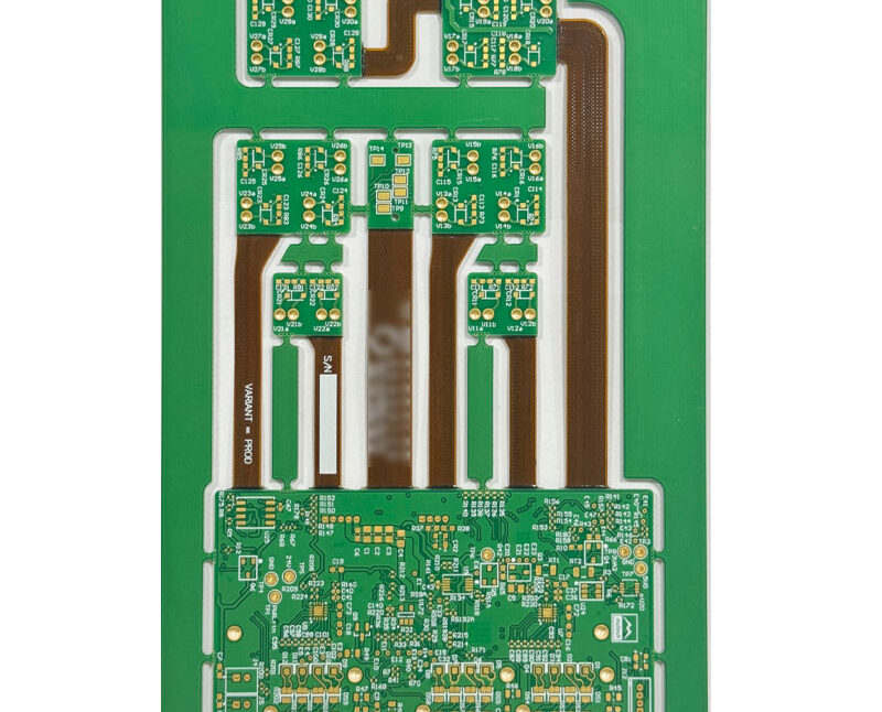
软硬结合板

Solder Mask Adhesion: Cure Verification and Tape Test Methods

  • By Frank guo
  • 2026年 9月 13日
  • PCB Assembly
  • No Comments
Solder Mask Adhesion: Cure Verification and Tape Test Methods A solder mask that is under-cured looks perfect until the board reaches a soldering temperature or a cleaning bath, and then it lifts from the copper or blisters off a trace. Cure and adhesion are the same question asked twice, and…
Continue Reading
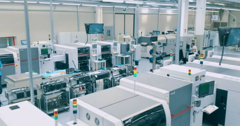
PCB Assembly Process

Microsection Preparation: Cutting, Mounting and Measuring Plated Barrels

  • By Frank guo
  • 2026年 9月 13日
  • PCB Assembly
  • No Comments
Microsection Preparation: Cutting, Mounting and Measuring Plated Barrels A microsection is the only check that shows what is inside a plated hole, and almost every error in the answer comes from the way the sample was made rather than from the way it was measured. Cutting, mounting and polishing each…
Continue Reading
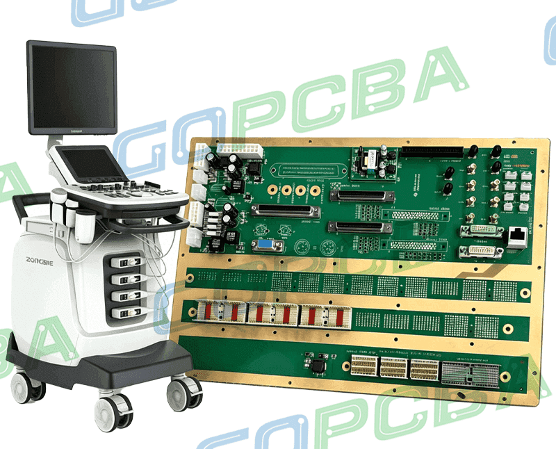
Ultrasound Diagnostic Device PCBA

Selective Soldering: Nozzle Wear, Flux Application and Pot Control

  • By Frank guo
  • 2026年 9月 13日
  • PCB Assembly
  • No Comments
Selective Soldering: Nozzle Wear, Flux Application and Pot Control Selective soldering replaces the wave for boards whose through-hole joints sit among tall surface mount parts, and it does so with a nozzle the size of a pencil. The process is governed by three things that wear or drift: the nozzle,…
Continue Reading
DSC_7375-1

Wave Solder Pallet Design: Fixtures, Shadowing and Through-Hole Fill

  • By Frank guo
  • 2026年 9月 13日
  • PCB Assembly
  • No Comments
Wave Solder Pallet Design: Fixtures, Shadowing and Through-Hole Fill A wave solder pallet carries the board across the wave, masks the side that must not be soldered and holds the assembly flat while it is hot. It also sits between the wave and the joint it is supposed to fill,…
Continue Reading
smart-home-PCBA

Reflow Carriers for Thin Boards: Support, Warp and Placement Accuracy

  • By Frank guo
  • 2026年 9月 13日
  • PCB Assembly
  • No Comments
Reflow Carriers for Thin Boards: Support, Warp and Placement Accuracy A board 0.6 mm thick with a large ball grid array on it will bend under its own weight as it crosses the oven, and the bending is what moves components after placement. A reflow carrier holds the panel flat…
Continue Reading
EV-System-Integration

Solder Paste Rheology: Viscosity, Metal Content and Printability

  • By Frank guo
  • 2026年 9月 13日
  • PCB Assembly
  • No Comments
Solder Paste Rheology: Viscosity, Metal Content and Printability A solder paste is a suspension of metal powder in flux, and the way that suspension flows decides whether the deposit is a clean brick or a smear. Viscosity is the single figure most often quoted, but it is only meaningful with…
Continue Reading
55387056_2

Laser Cut Stencil: Design Rules and Process Limits

  • By Frank guo
  • 2026年 9月 13日
  • PCB Assembly
  • No Comments
Laser Cut Stencil: Design Rules and Process Limits Two stencils with the same aperture sizes can deposit different volumes, because the volume depends on the shape of the aperture wall as much as on its dimensions. A laser cut stencil and an electroformed stencil reach the same geometry by different…
Continue Reading
55387056_2

Paste in Hole: Reflowing Through-Hole Connectors With Printed Paste

  • By Frank guo
  • 2026年 9月 13日
  • PCB Assembly
  • No Comments
Paste in Hole: Reflowing Through-Hole Connectors With Printed Paste Paste in hole prints solder into the barrel of a through-hole part and reflows it in the same pass as the surface mount devices, which removes a wave soldering step and the handling that goes with it. It works only when…
Continue Reading
1 … 540 541 542 … 1,621

Search Posts

Categories

  • Electronic Materials
  • Electronical Engineering
  • Industrial Control
  • PCB Assembly
  • PCB Design
  • PCB Manufacturing

Recent Posts

Low-Temperature Solder for LED Modules: Thermal Budget and Joint Reliability

Frank guo - 2026年 11月 6日
Surface Mount Technology (SMT): Process, Components, Design Guidelines & PCB Assembly

Surface Mount Technology (SMT): Process, Components, Design Guidelines & PCB Assembly

Zane Zhang - 2026年 10月 2日
Cheap PCB Costs: PCB Design, PCB Manufacturing & SMT vs TH Guide

Cheap PCB Costs: PCB Design, PCB Manufacturing & SMT vs TH Guide

Jelly - 2026年 9月 30日

Tags

AOI inspection automotive electronics automotive PCBA quality automotive standards box build assembly component procurement component supplier conformal coating defect prevention DFM checks DFM review e-bom management electronic component shortage electronic manufacturing services electronic manufacturing standards Electronic Materials electronics design best practice electronics manufacturing capacity electronics sourcing high volume production industrial electronics manufacturability review mass production quality mixed technology PCB PCBA inspection PCBA prototype PCBA turnkey PCBA volume pricing PCB Design PCB layout rules PCB Manufacturing PCB sourcing power electronics PCB printed circuit board prototype quick turn PCB reflow soldering reflow soldering profile SMT assembly quality SMT production soldering defect analysis solder joint quality solder paste inspection solder paste printing surface mount technology vehicle electronics
GOPCBA-logo

As a professional China PCB assembly manufacturer, we provide a full range of electronic manufacturing services from PCB fabrication, PCBA to OEM/ODM, including PCB design, PCB layout, rapid PCBA prototyping, components procurement, SMT/ THT assembly, china pcb assembly, china pcb prototype, PCBA testing and box build assembly.

Linkedin Facebook-f X-twitter Youtube Instagram

PCB ASSEMBLY

  • Prototype PCB Assembly
  • Low Volume PCB Assembly
  • High Volume PCB Assembly
  • Turnkey PCB Assembly
  • SMT PCB Assembly
  • Through Hole PCB Assembly
  • Mixed Technology PCB Assembly
  • Flex PCB Assembly

OUR SERVICES

  • PCB Design/Layout
  • PCB Manufacturing
  • Rapid PCBA Prototyping
  • Components Procurement
  • Conformal Coating
  • PCBA Testing
  • Box Build Assembly
  • Wire & Cable Harness Assembly

TECHNICAL SUPPORT

  • About Us
  • Quality Management
  • Artificial Intelligence PCBA
  • Industrial PCBA
  • IOT PCBA
  • Medical PCBA
  • Energy PCBA
  • Telecommunications PCBA

Copyright © 2026. Shenzhen Kingda Electronics Co., LTD  All rights reserved. 

  • Sitemap
  • Terms of Service
  • Privacy Policy
Zmdi Zmdi-email Phone-square Whatsapp Weixin
x

ABOUT US

Progressively maintain extensive infomediaries via extensible nich. Capitalize on low hanging fruit. a ballpark value added is activity to beta test. Override the digital divide with additional click throughs from fruit.

LOCATIONS

map

Shenzhen Office

+86-181-2376-9076
sales@gopcba.com
3rd Floor, Building 11, Houting Third Industrial Zone, Shajing Avenue, Baoan District, Shenzhen, China.
Contact Us

FOLLOW US